SNOS674J October   1997  – September 2024 LMC6482 , LMC6484

PRODUCTION DATA  

  1.   1
  2. Features
  3. Applications
  4. Description
  5. Pin Configuration and Functions
  6. Specifications
    1. 5.1 Absolute Maximum Ratings
    2. 5.2 ESD Ratings
    3. 5.3 Recommended Operating Conditions
    4. 5.4 Thermal Information LMC6482
    5. 5.5 Thermal Information LMC6484
    6. 5.6 Electrical Characteristics: VS = 5V
    7. 5.7 Electrical Characteristics: VS = 3V
    8. 5.8 Typical Characteristics
  7. Detailed Description
    1. 6.1 Overview
    2. 6.2 Functional Block Diagram
    3. 6.3 Feature Description
      1. 6.3.1 Amplifier Topology
      2. 6.3.2 Input Common-Mode Voltage Range
      3. 6.3.3 Rail-to-Rail Output
    4. 6.4 Device Functional Modes
  8. Application and Implementation
    1. 7.1 Application Information
      1. 7.1.1 Upgrading Applications
      2. 7.1.2 Data Acquisition Systems
      3. 7.1.3 Instrumentation Circuits
    2. 7.2 Typical Applications
      1. 7.2.1 3V Single-Supply Buffer Circuit
        1. 7.2.1.1 Design Requirements
        2. 7.2.1.2 Detailed Design Procedure
          1. 7.2.1.2.1 Capacitive Load Compensation
          2. 7.2.1.2.2 Capacitive Load Tolerance
          3. 7.2.1.2.3 Compensating For Input Capacitance
          4. 7.2.1.2.4 Offset Voltage Adjustment
        3. 7.2.1.3 Application Curves
      2. 7.2.2 Typical Single-Supply Applications
    3. 7.3 Power Supply Recommendations
    4. 7.4 Layout
      1. 7.4.1 Layout Guidelines
      2. 7.4.2 Layout Example
  9. Device and Documentation Support
    1. 8.1 Device Support
      1. 8.1.1 Development Support
        1. 8.1.1.1 Spice Macromodel
        2. 8.1.1.2 PSpice® for TI
        3. 8.1.1.3 TINA-TI™ Simulation Software (Free Download)
        4. 8.1.1.4 DIP-Adapter-EVM
        5. 8.1.1.5 DIYAMP-EVM
        6. 8.1.1.6 TI Reference Designs
        7. 8.1.1.7 Analog Filter Designer
    2. 8.2 Receiving Notification of Documentation Updates
    3. 8.3 Support Resources
    4. 8.4 Trademarks
    5. 8.5 Electrostatic Discharge Caution
    6. 8.6 Glossary
  10. Revision History
  11. 10Mechanical, Packaging, and Orderable Information
Capacitive Load Tolerance

The LMC648x can typically directly drive a 100pF load with VS = 15V at unity gain without oscillating. The unity gain follower is the most sensitive configuration. Direct capacitive loading reduces the phase margin of op amps. The combination of the output impedance of the op-amp and the capacitive load induces phase lag. This results in either an underdamped pulse response or oscillation.

Figure 7-10 shows how improved frequency response is achieved by indirectly driving capacitive loads.

LMC6482  LMC6484 LMC648x Noninverting Amplifier
NOTE: Compensated to handle a 330pF capacitive load.
Figure 7-10 LMC648x Noninverting Amplifier

R1 and C1 serve to counteract the loss of phase margin by feeding forward the high-frequency component of the output signal back to the amplifiers inverting input, thereby preserving phase margin in the overall feedback loop. The values of R1 and C1 are experimentally determined for the desired pulse response. Figure 7-11 shows the resulting pulse response.
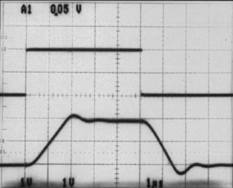
LMC6482  LMC6484 Pulse Response of LMC6482
                    Circuit in Figure 7-10 Figure 7-11 Pulse Response of LMC6482 Circuit in Figure 7-10