SNOS674J October 1997 – September 2024 LMC6482 , LMC6484
PRODUCTION DATA
- 1
- 1 Features
- 2 Applications
- 3 Description
- 4 Pin Configuration and Functions
- 5 Specifications
- 6 Detailed Description
- 7 Application and Implementation
- 8 Device and Documentation Support
- 9 Revision History
- 10Mechanical, Packaging, and Orderable Information
5.8 Typical Characteristics
at VS = 15V, single supply, and TA = 25°C (unless otherwise specified)
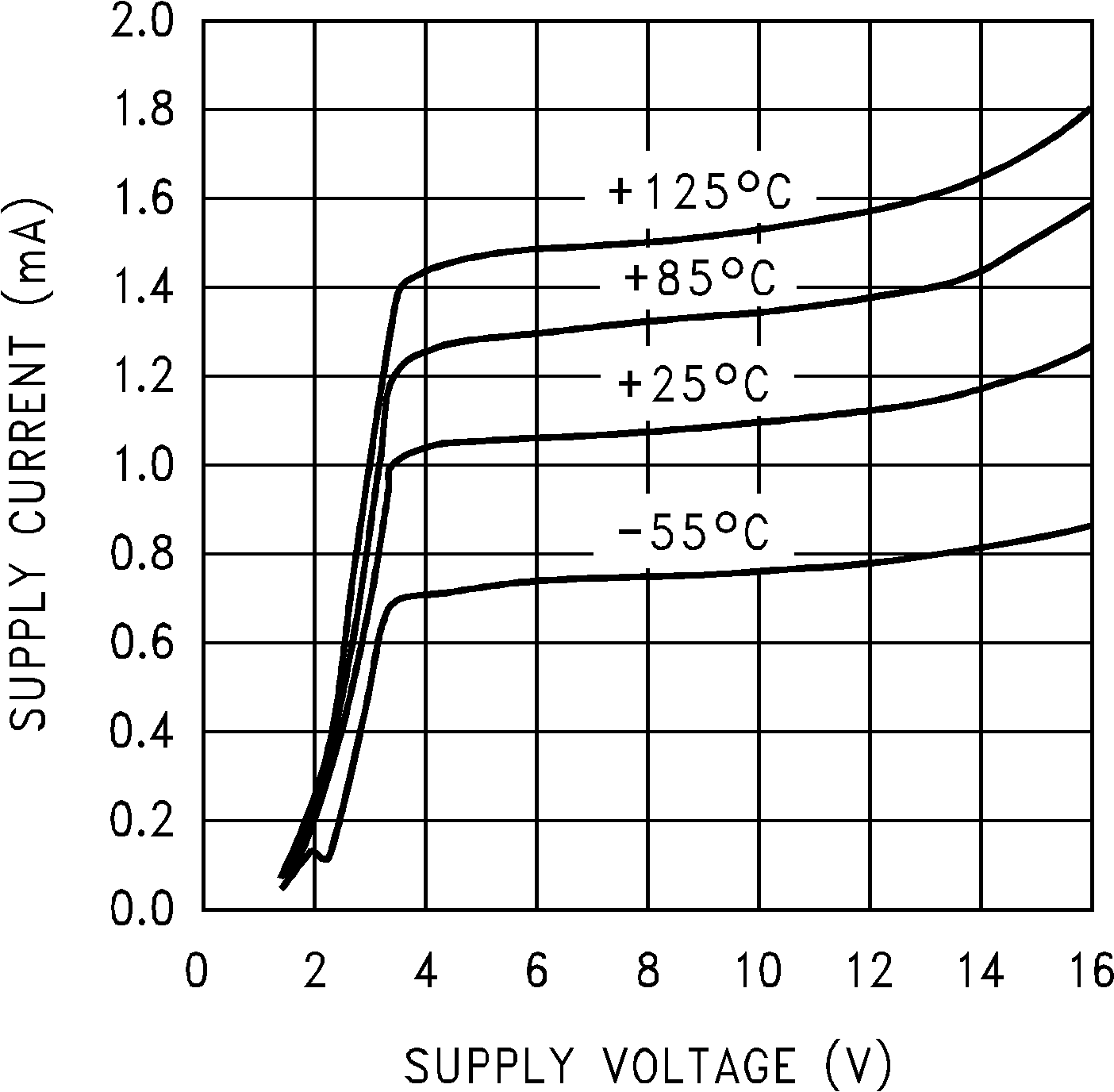 Figure 5-1 Supply Current vs Supply Voltage
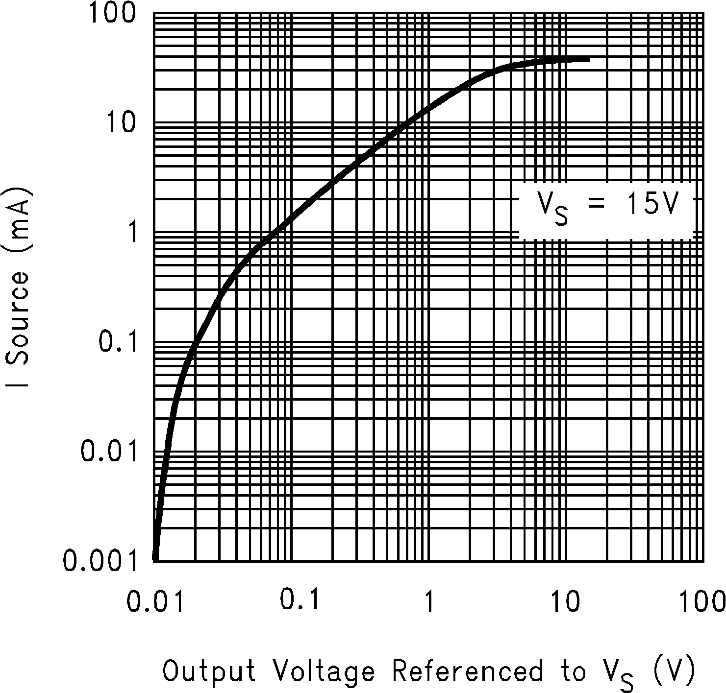 Figure 5-3 Sourcing Current vs Output Voltage
 Figure 5-5 Sourcing Current vs Output Voltage
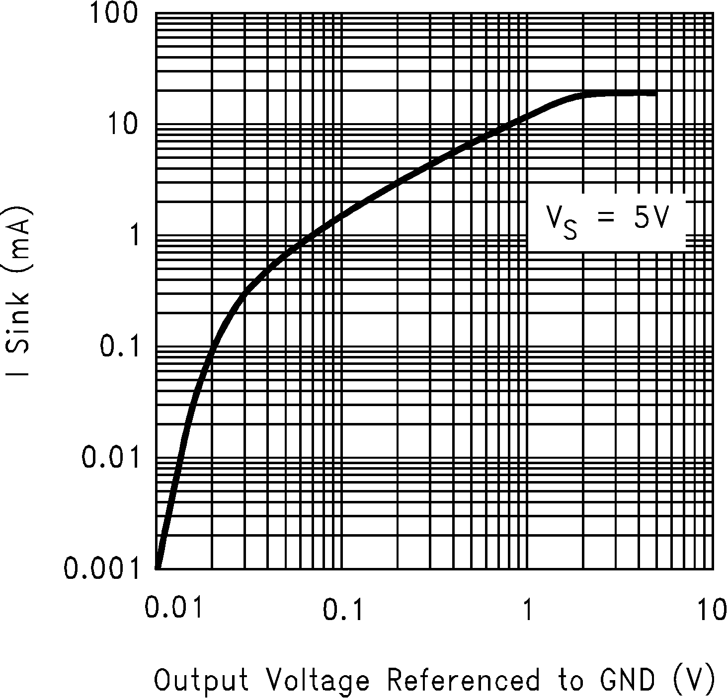 Figure 5-7 Sinking Current vs Output Voltage
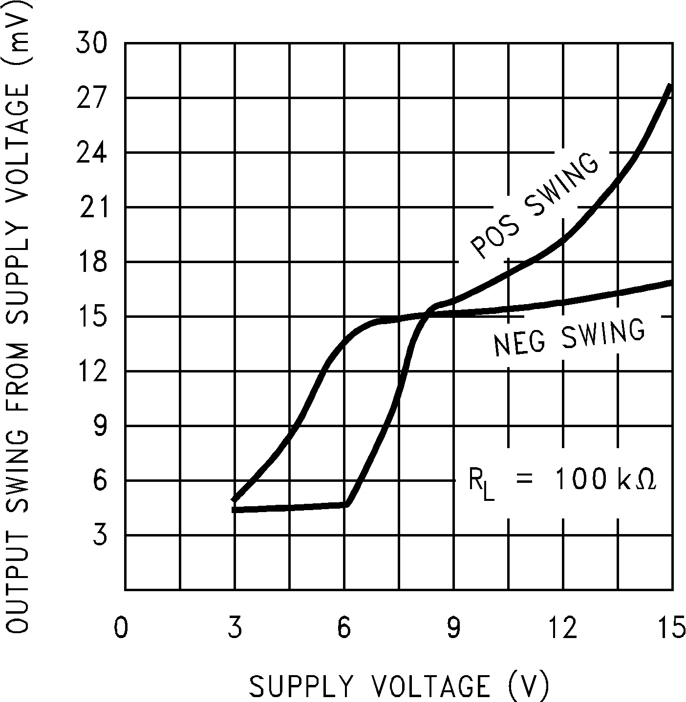 Figure 5-9 Output Voltage Swing vs Supply Voltage
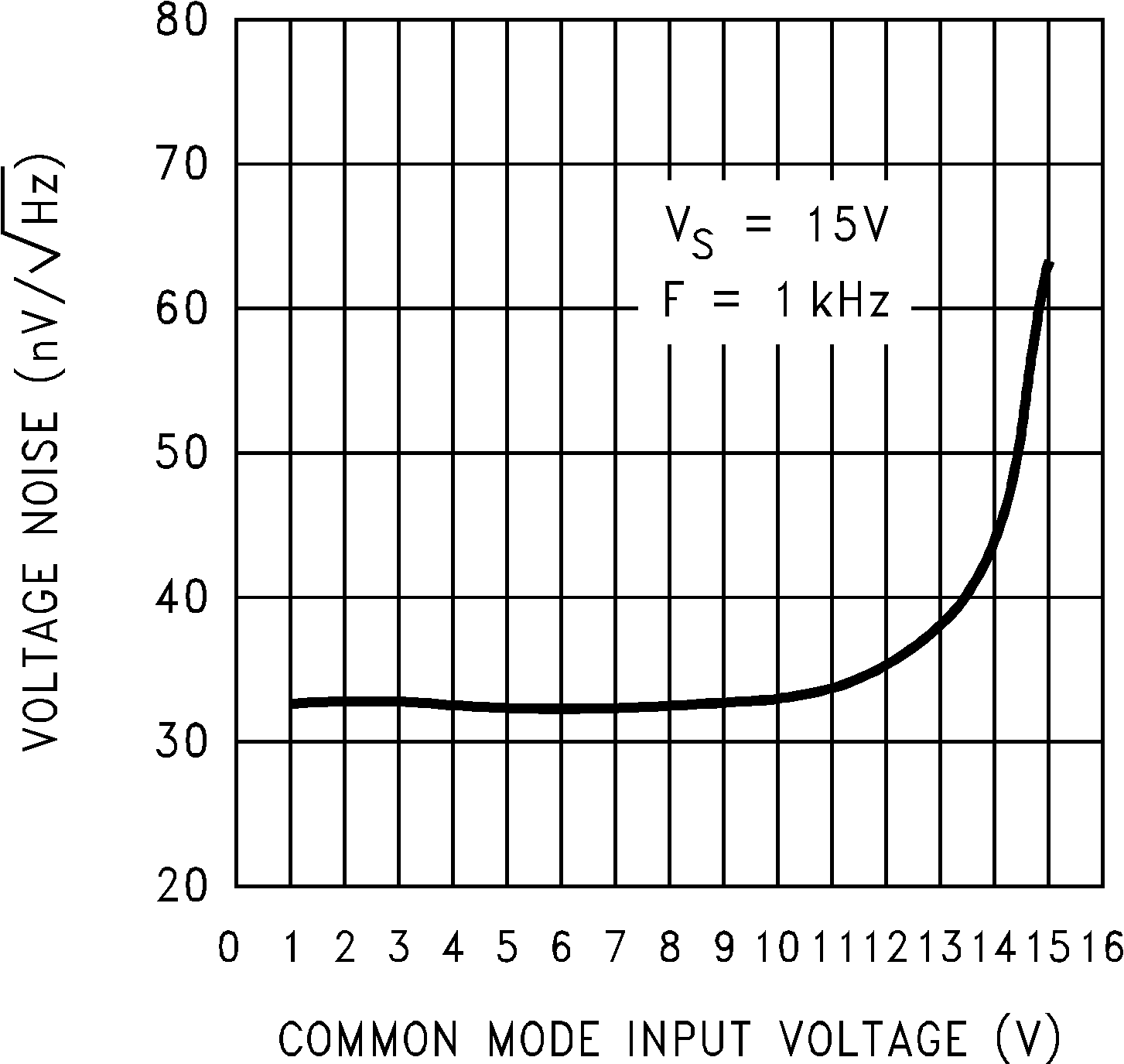 Figure 5-11 Input
Voltage Noise vs Input Voltage
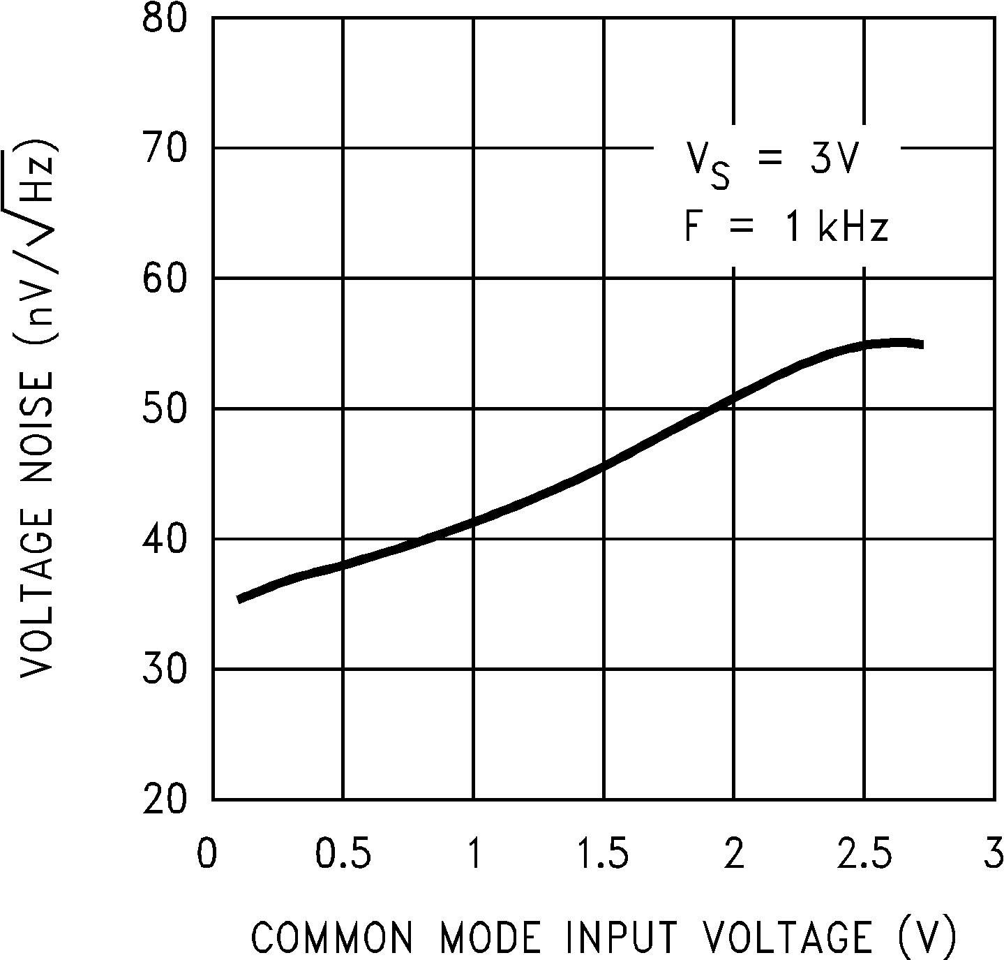 Figure 5-13 Input
Voltage Noise vs Input Voltage
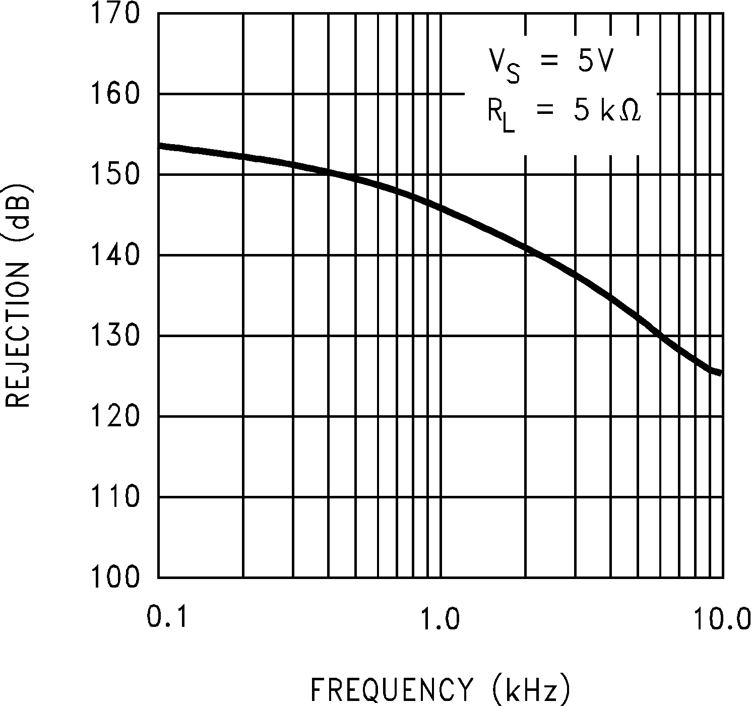 Figure 5-15 Crosstalk Rejection vs Frequency
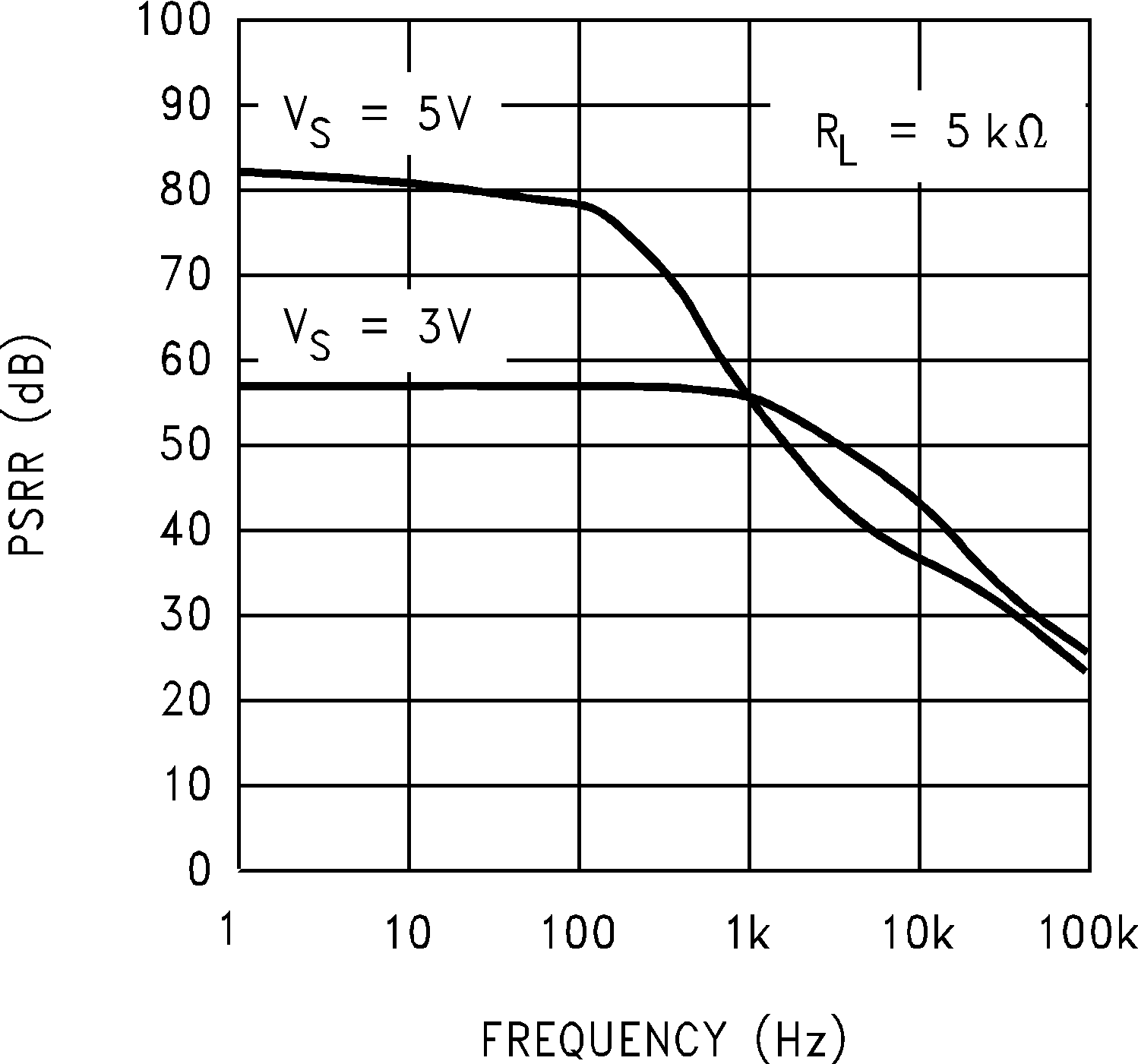 Figure 5-17 Negative PSRR vs Frequency
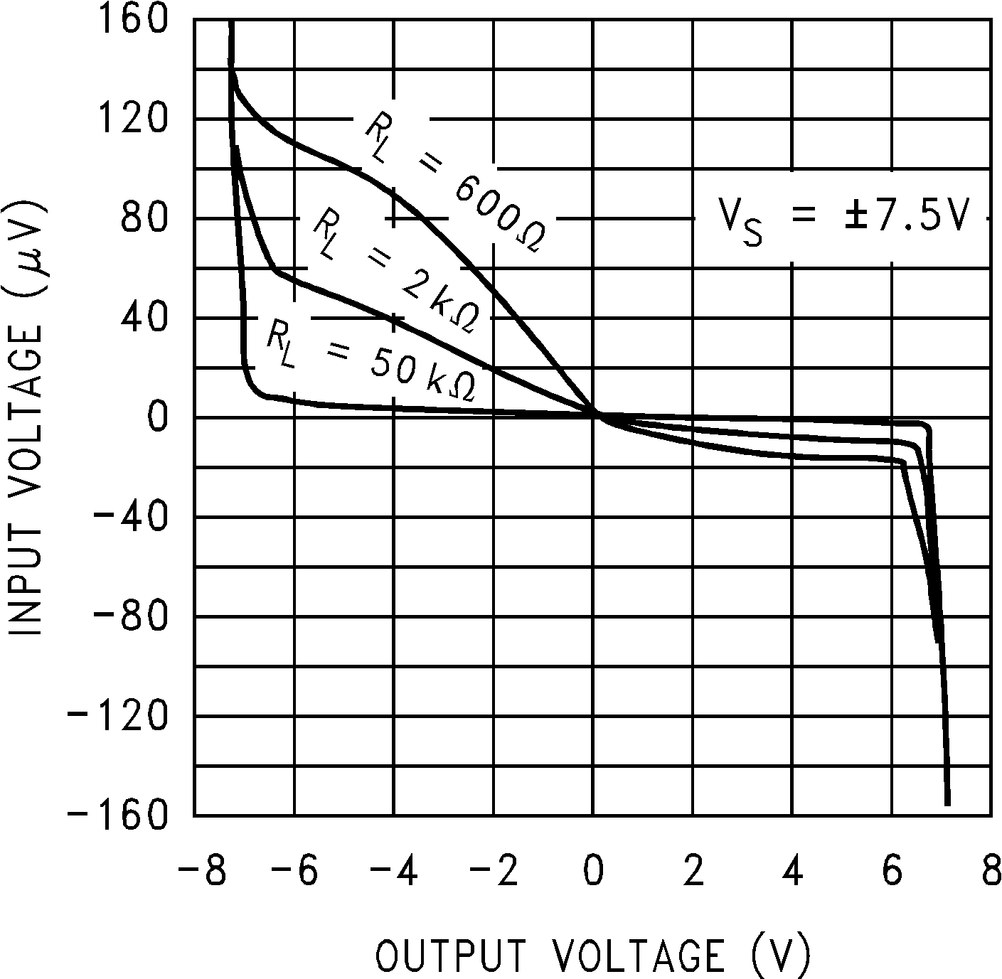 Figure 5-19 Input
Voltage vs Output Voltage
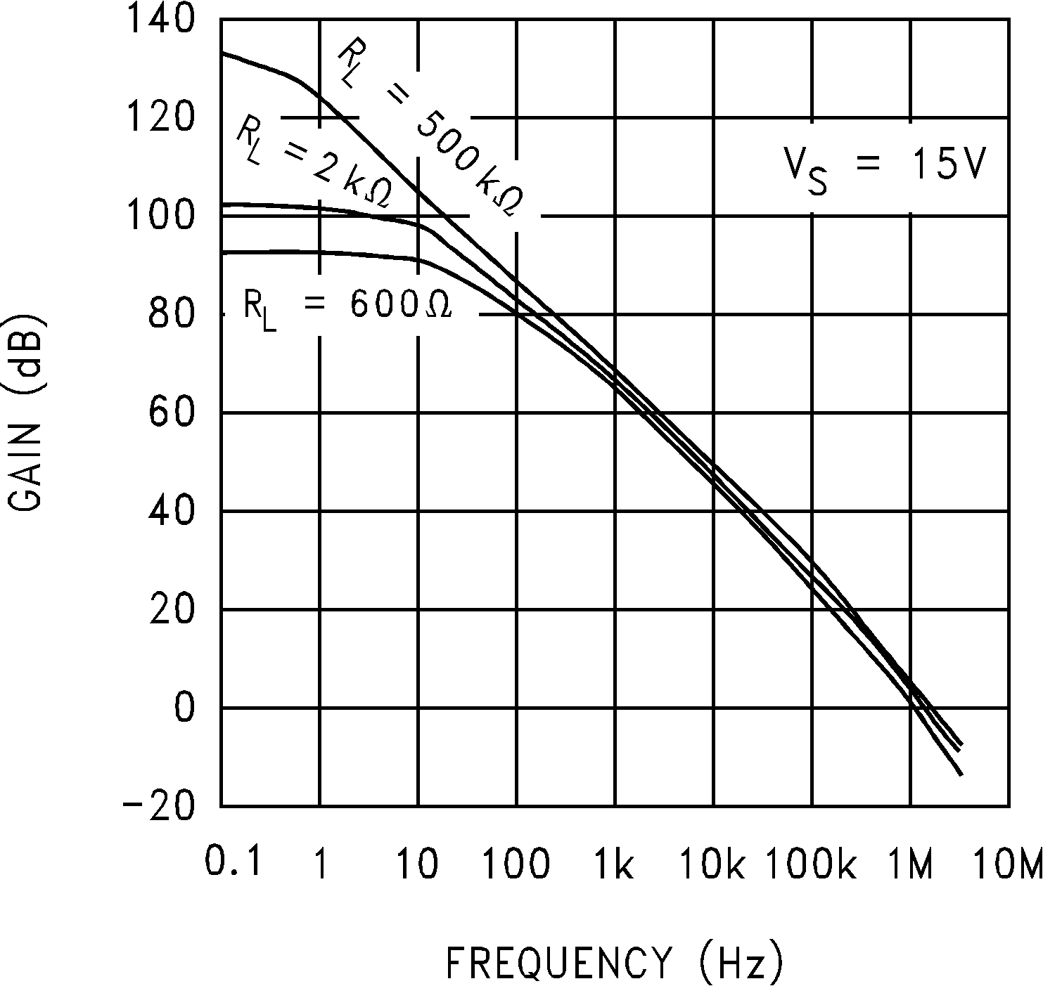 Figure 5-21 Open-Loop Frequency Response
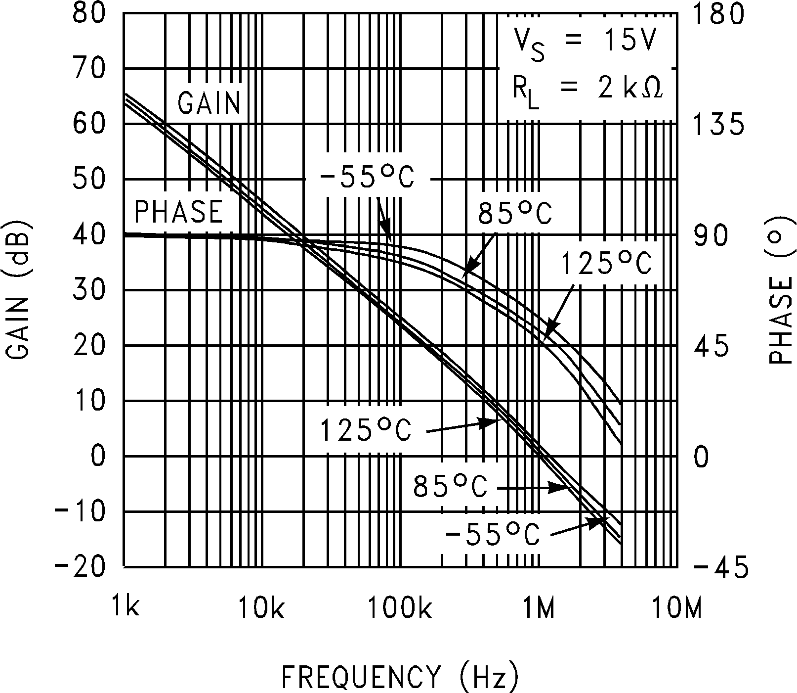 Figure 5-23 Open-Loop Frequency Response vs Temperature
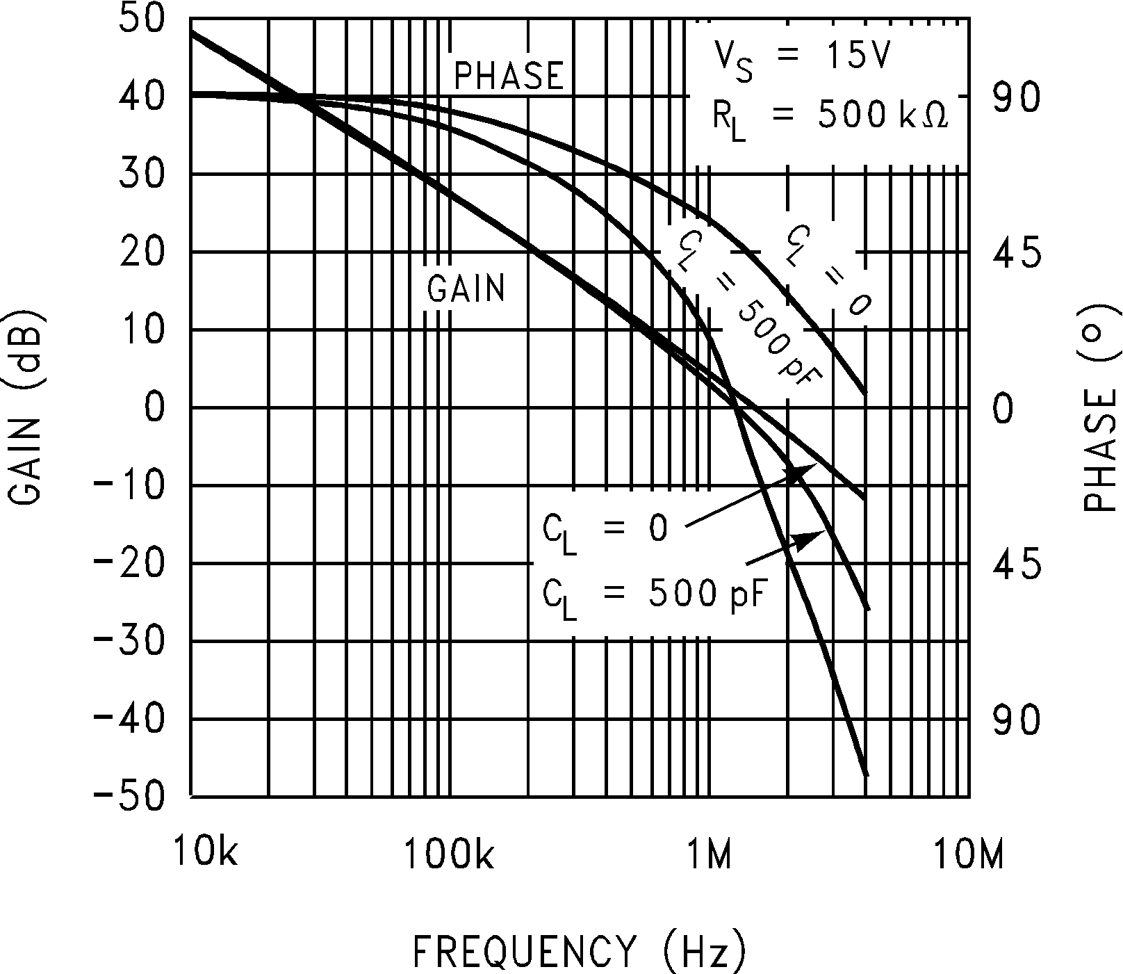 Figure 5-25 Gain
and Phase vs Capacitive Load
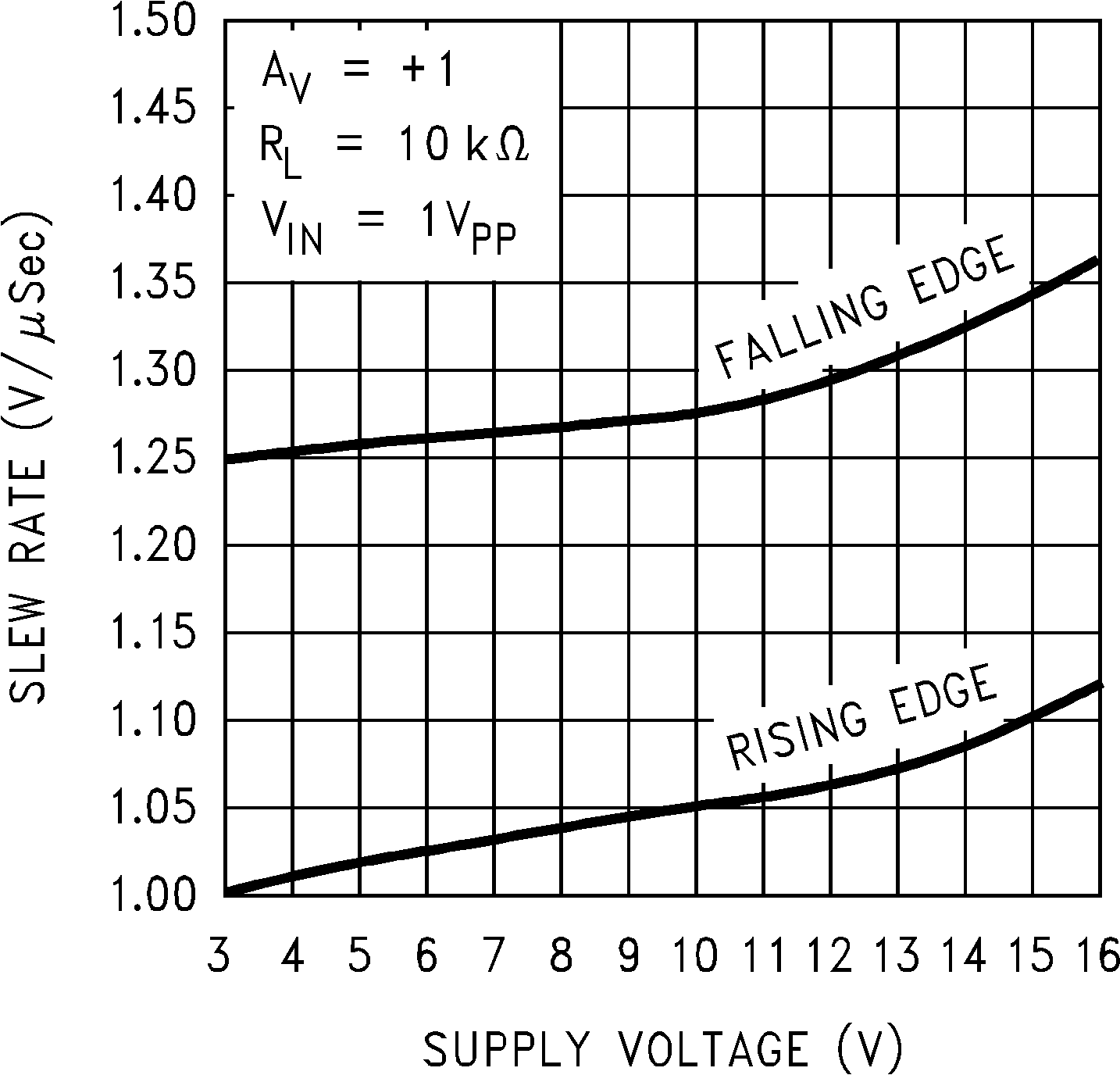 Figure 5-27 Slew
Rate vs Supply Voltage
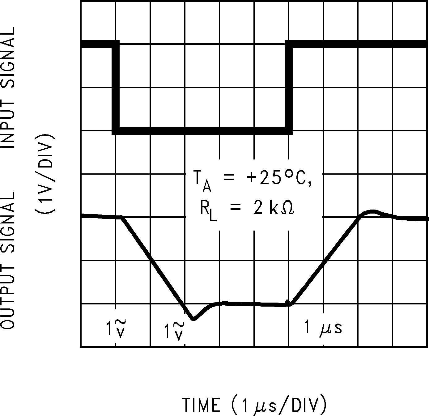 Figure 5-29 Noninverting Large Signal Pulse Response
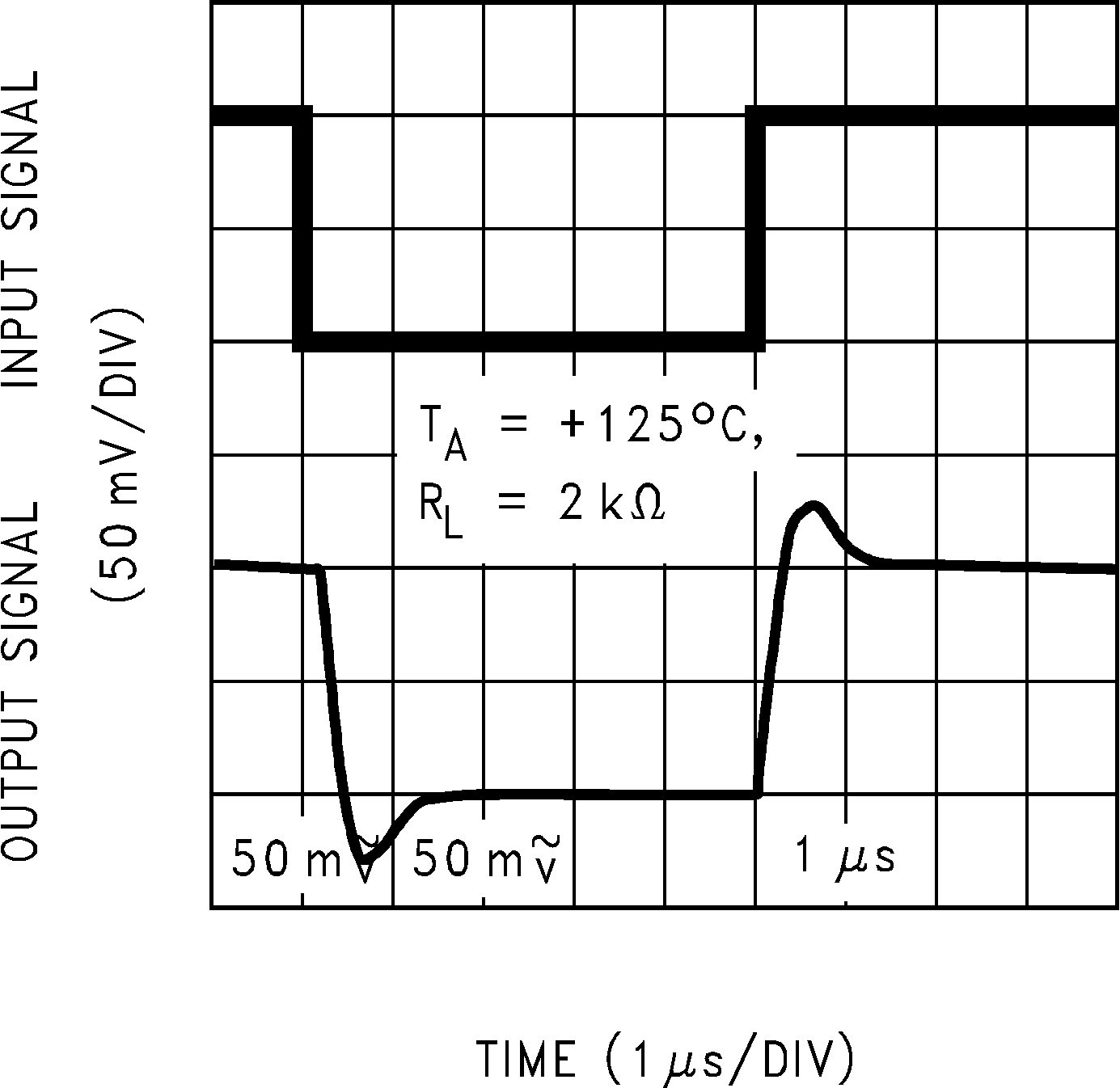 Figure 5-31 Noninverting Small Signal Pulse Response
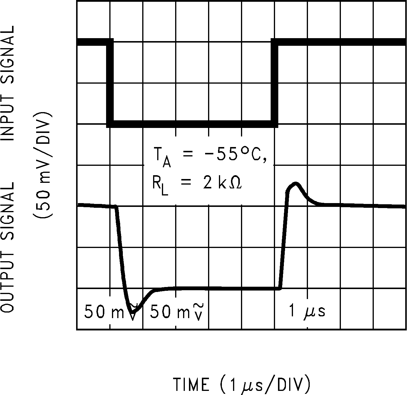 Figure 5-33 Noninverting Small Signal Pulse Response
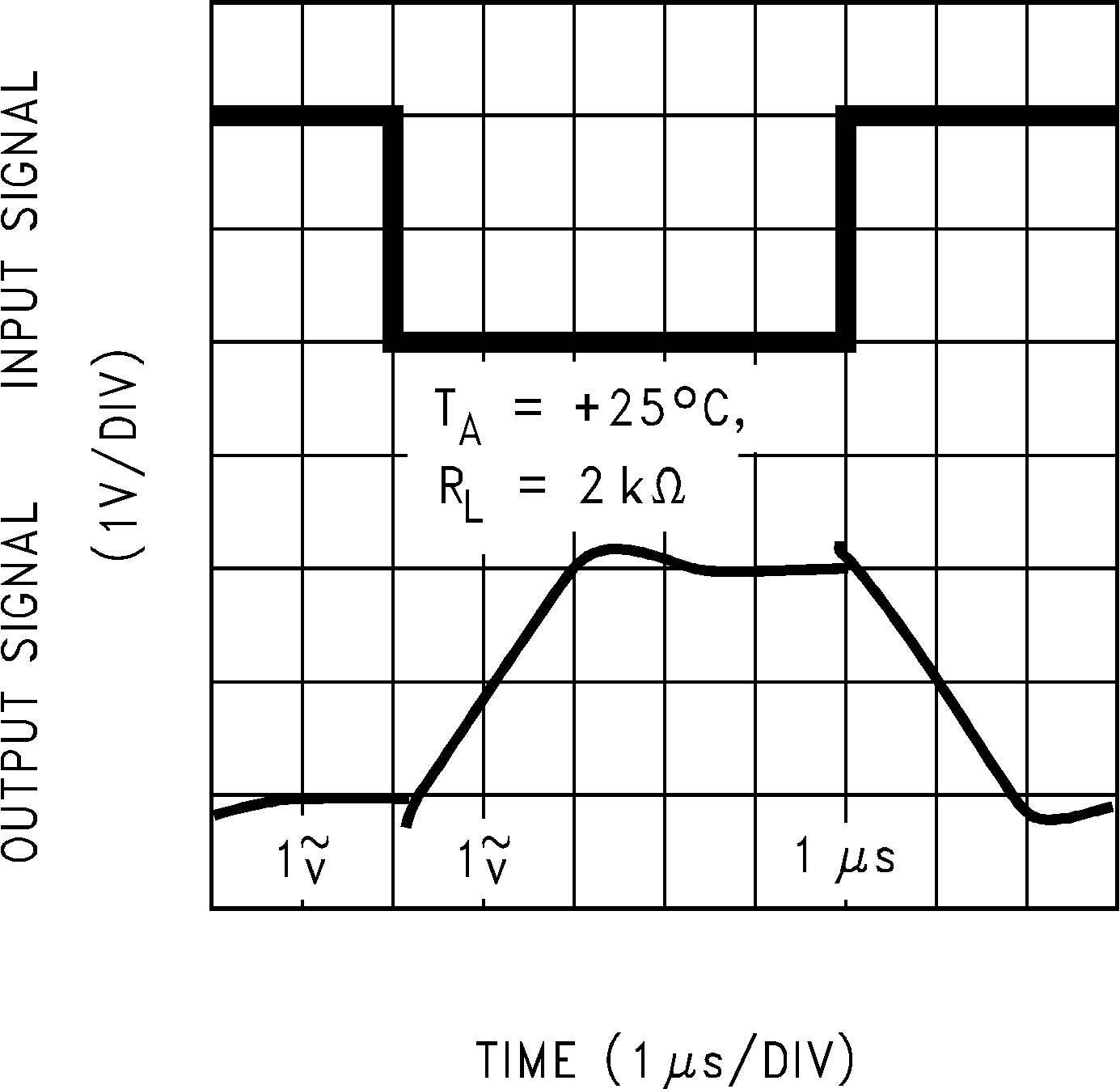 Figure 5-35 Inverting Large Signal Pulse Response
 Figure 5-37 Inverting Small Signal Pulse Response
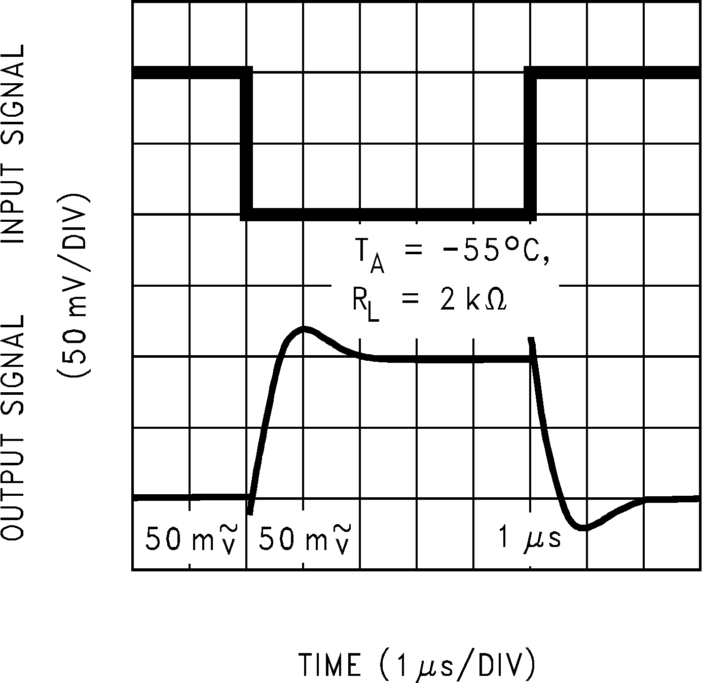 Figure 5-39 Inverting Small Signal Pulse Response
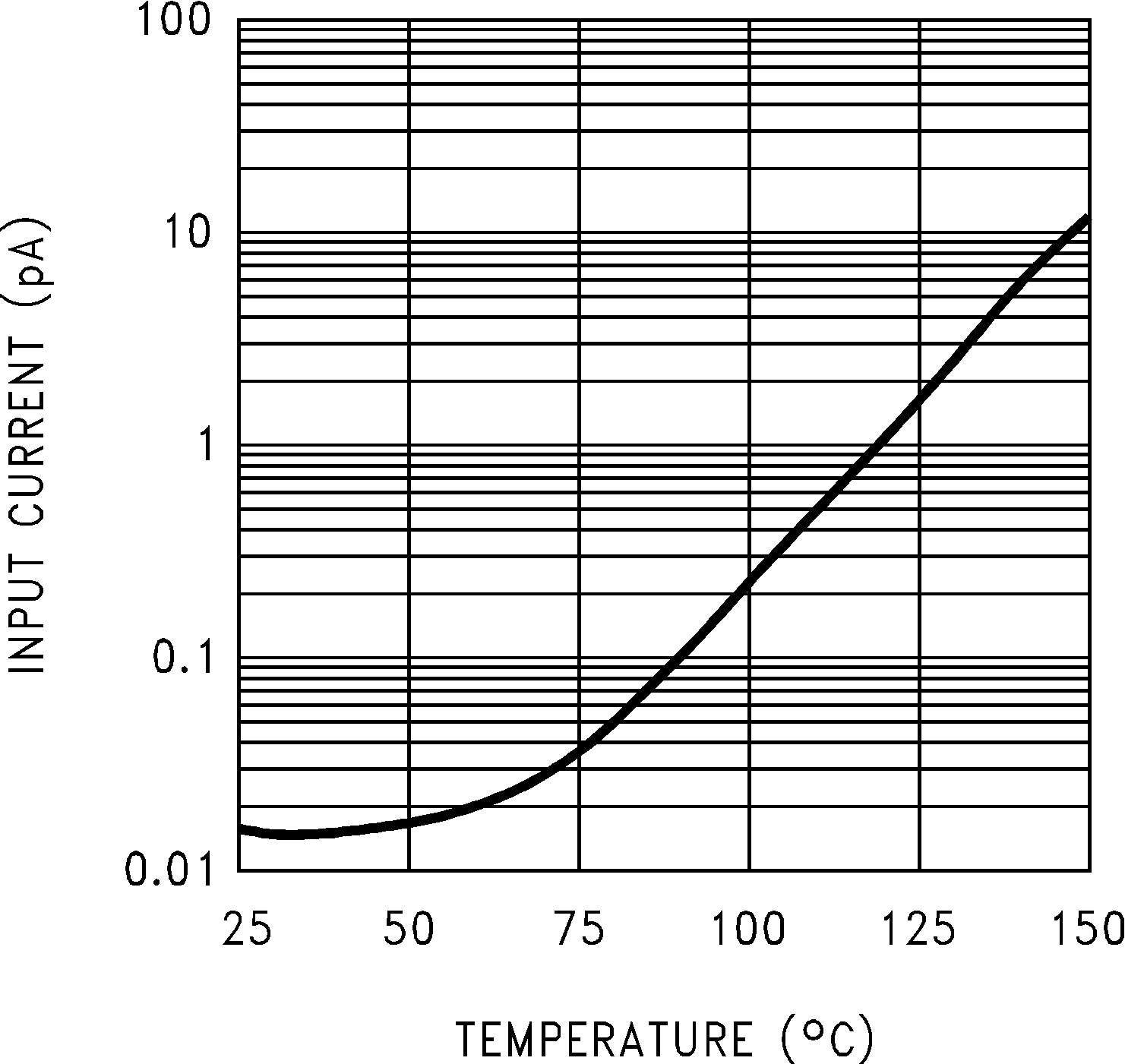 Figure 5-2 Input
Current vs Temperature
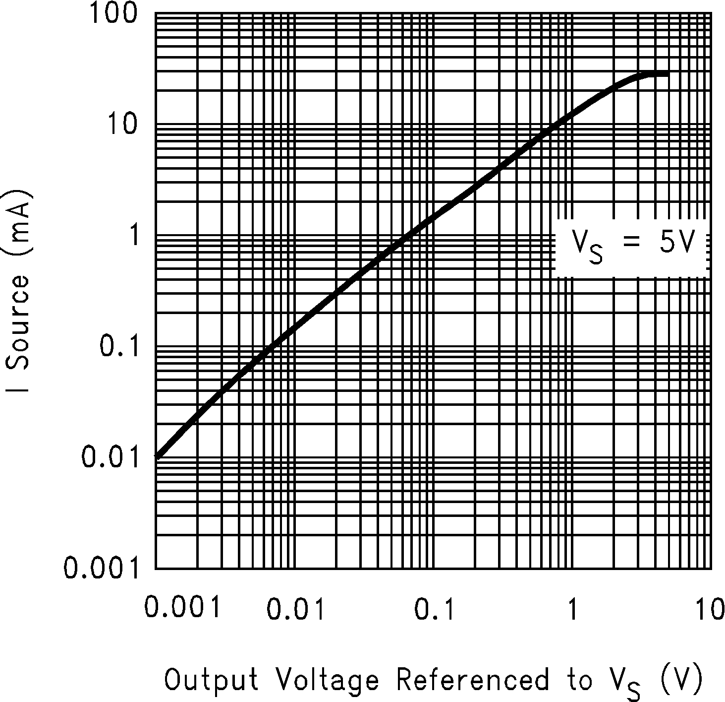 Figure 5-4 Sourcing Current vs Output Voltage
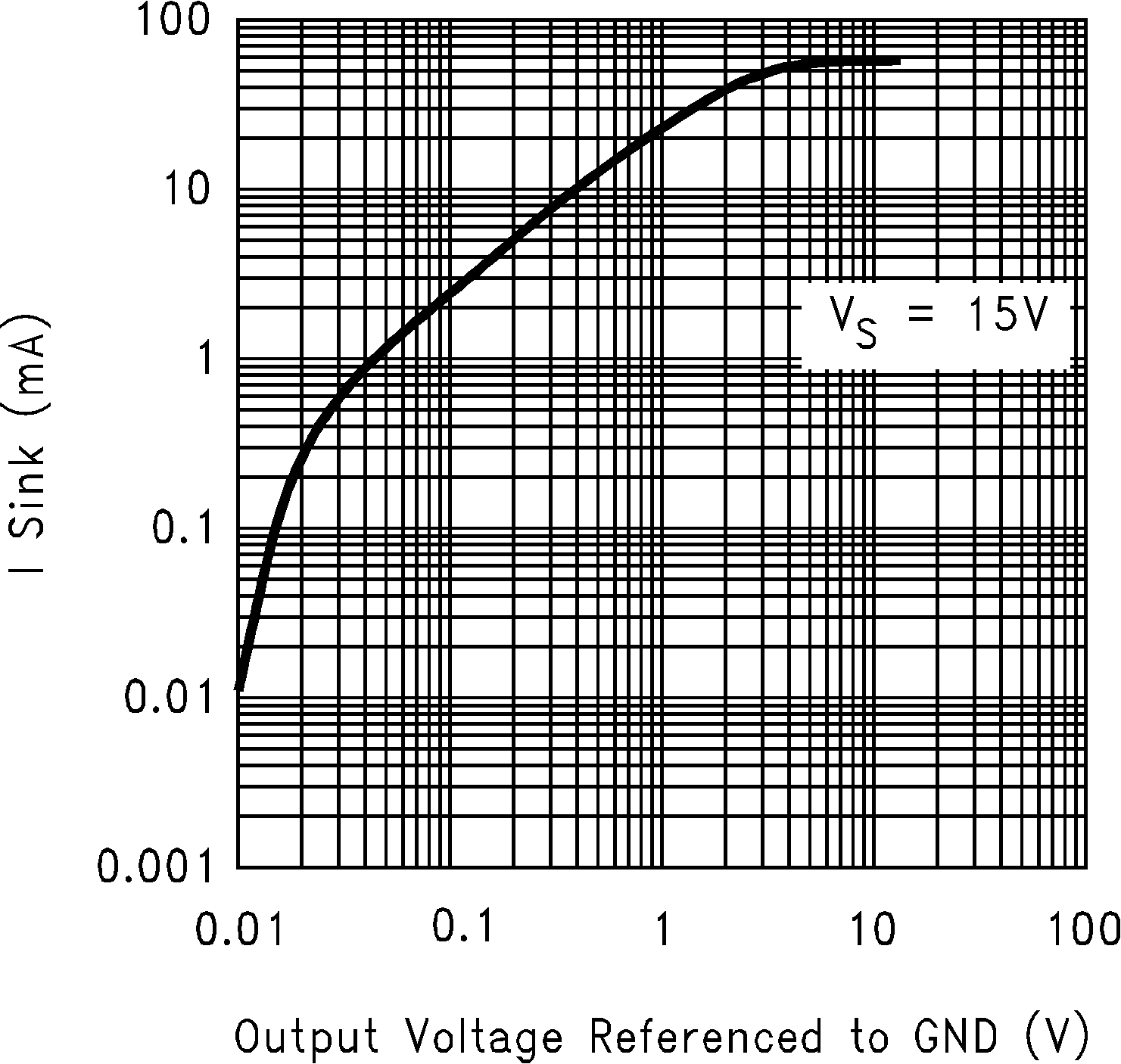 Figure 5-6 Sinking Current vs Output Voltage
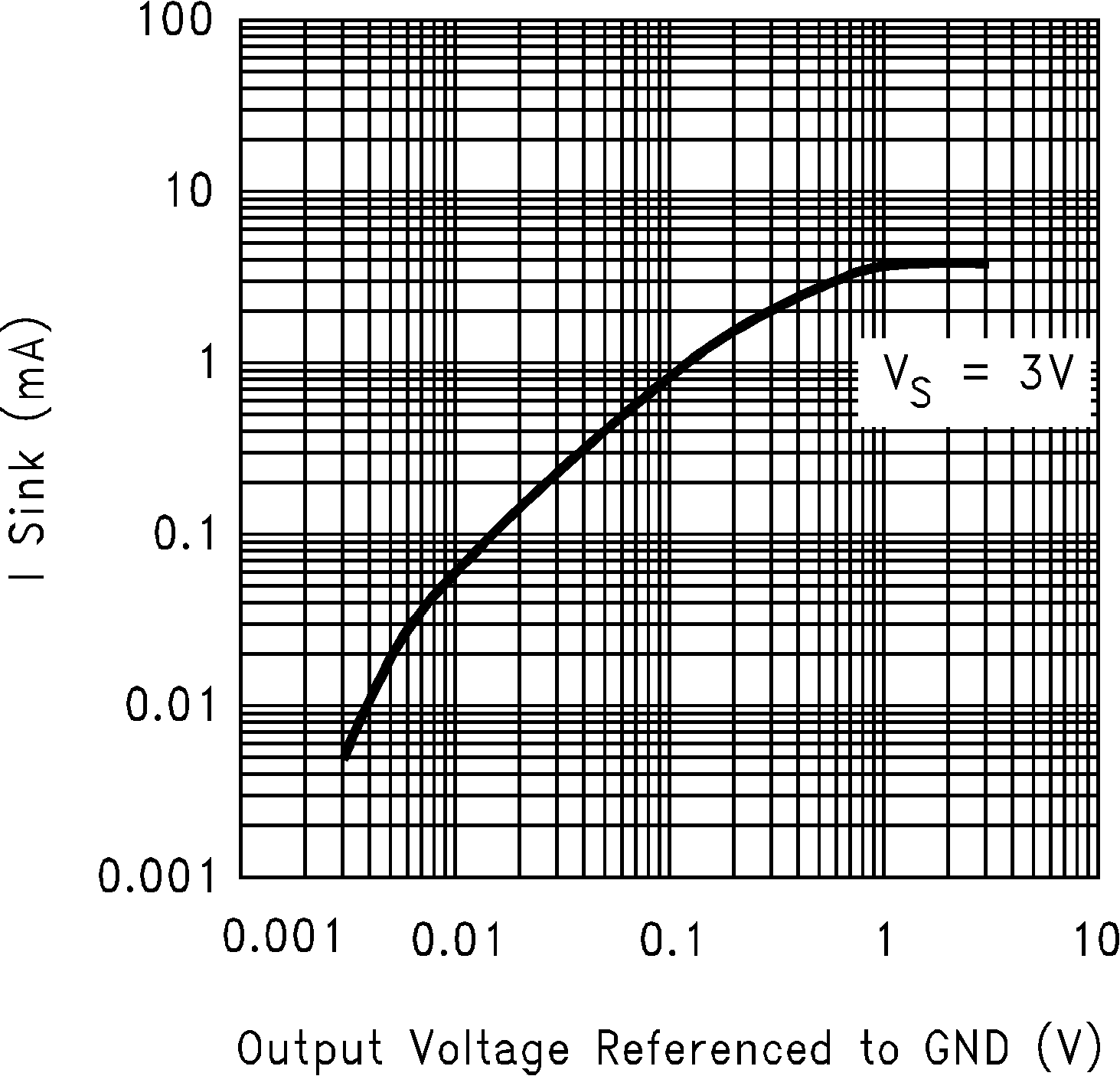 Figure 5-8 Sinking Current vs Output Voltage
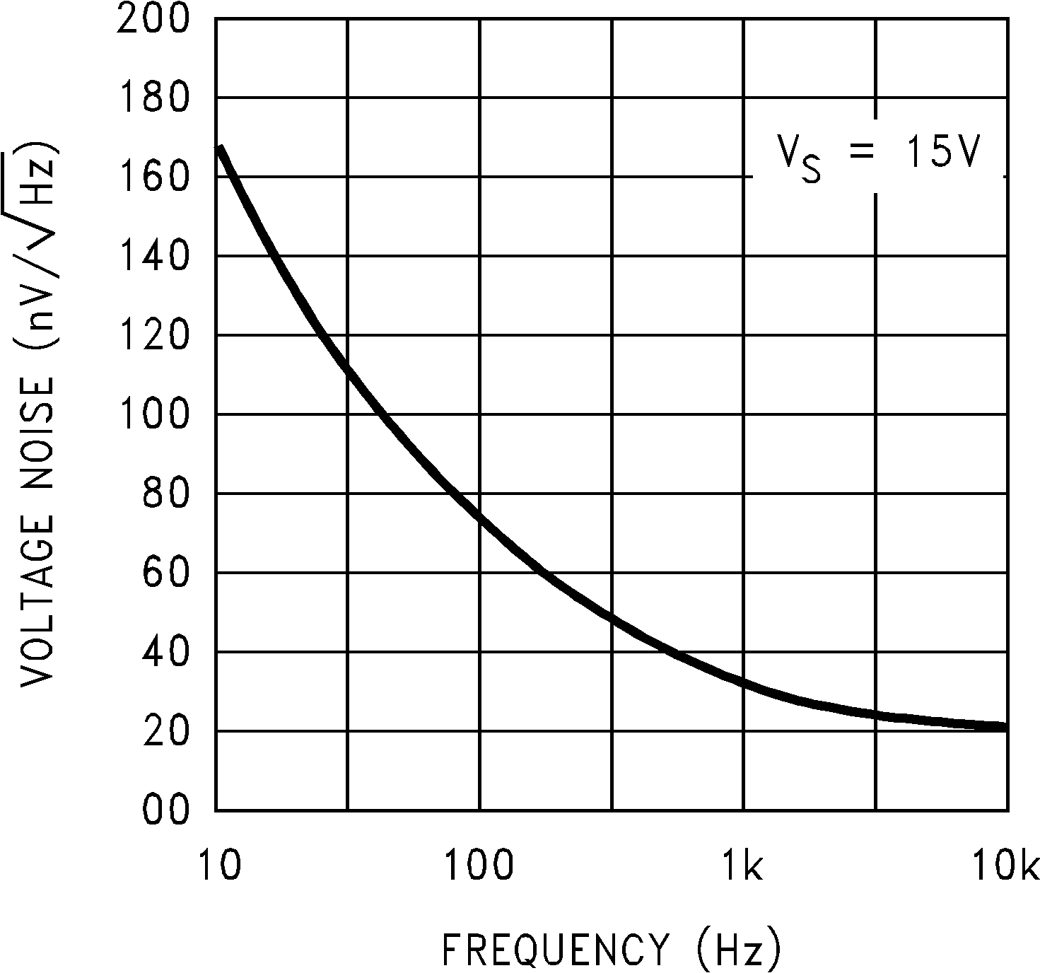 Figure 5-10 Input
Voltage Noise vs Frequency
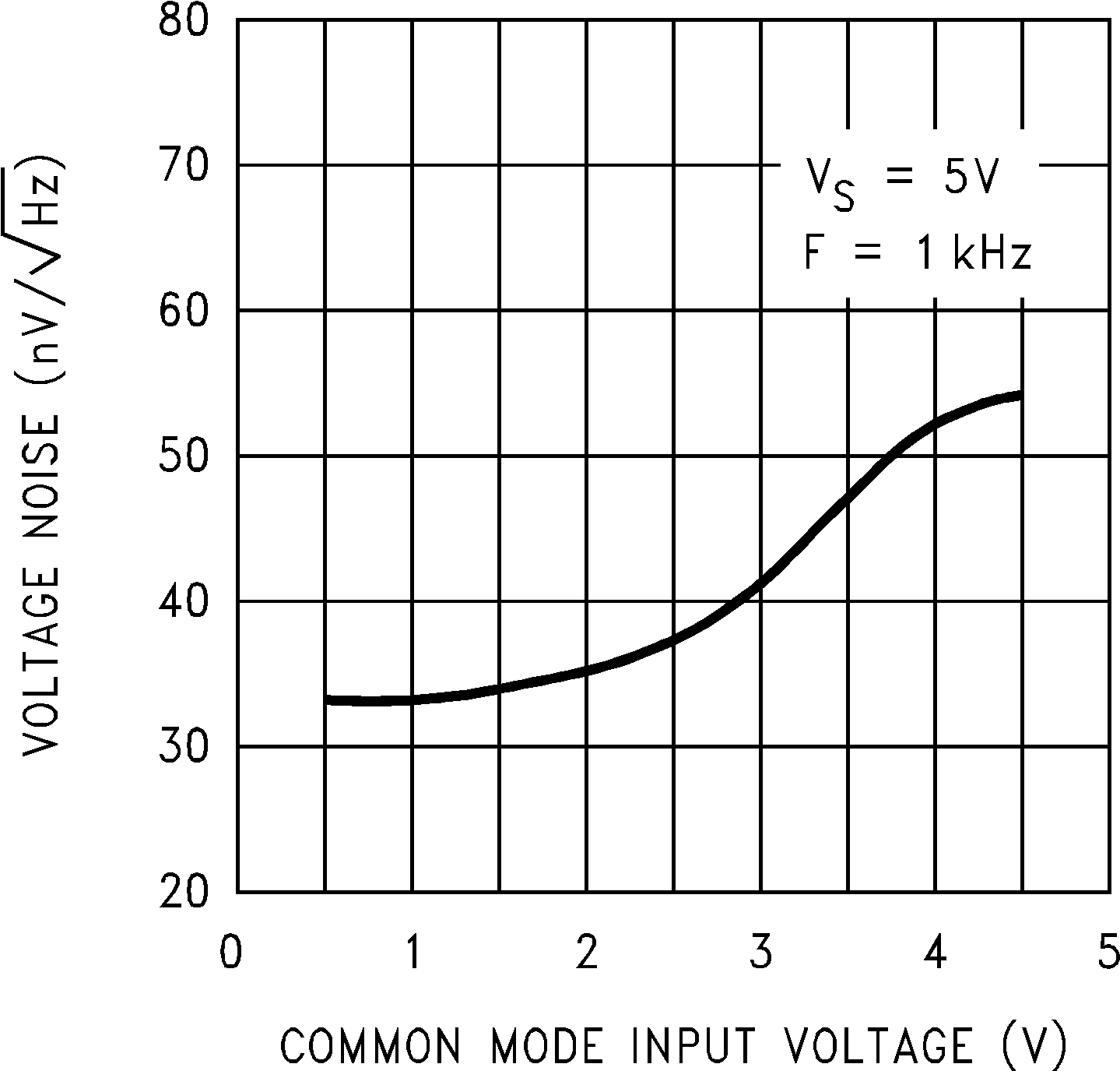 Figure 5-12 Input
Voltage Noise vs Input Voltage
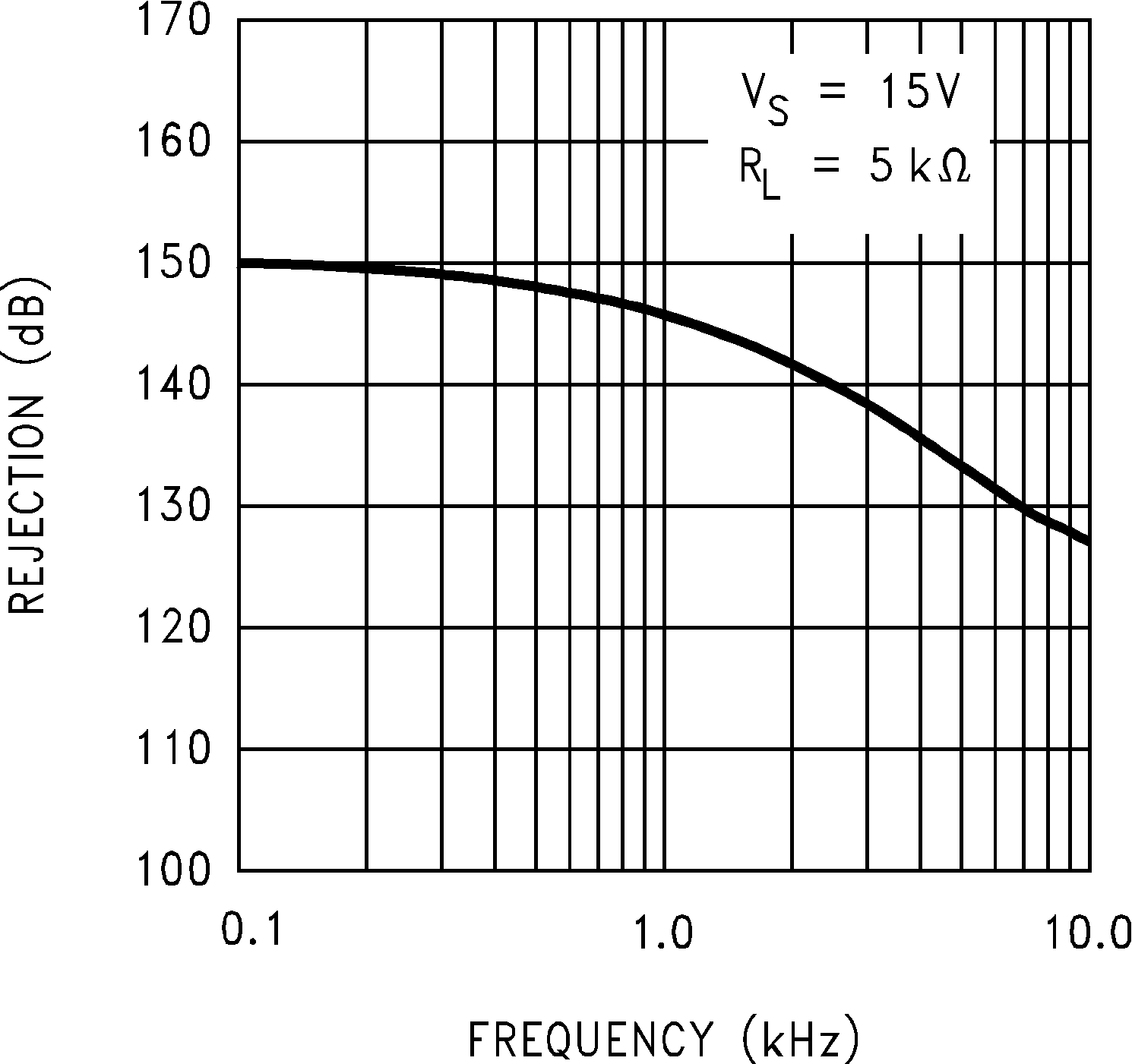 Figure 5-14 Crosstalk Rejection vs Frequency
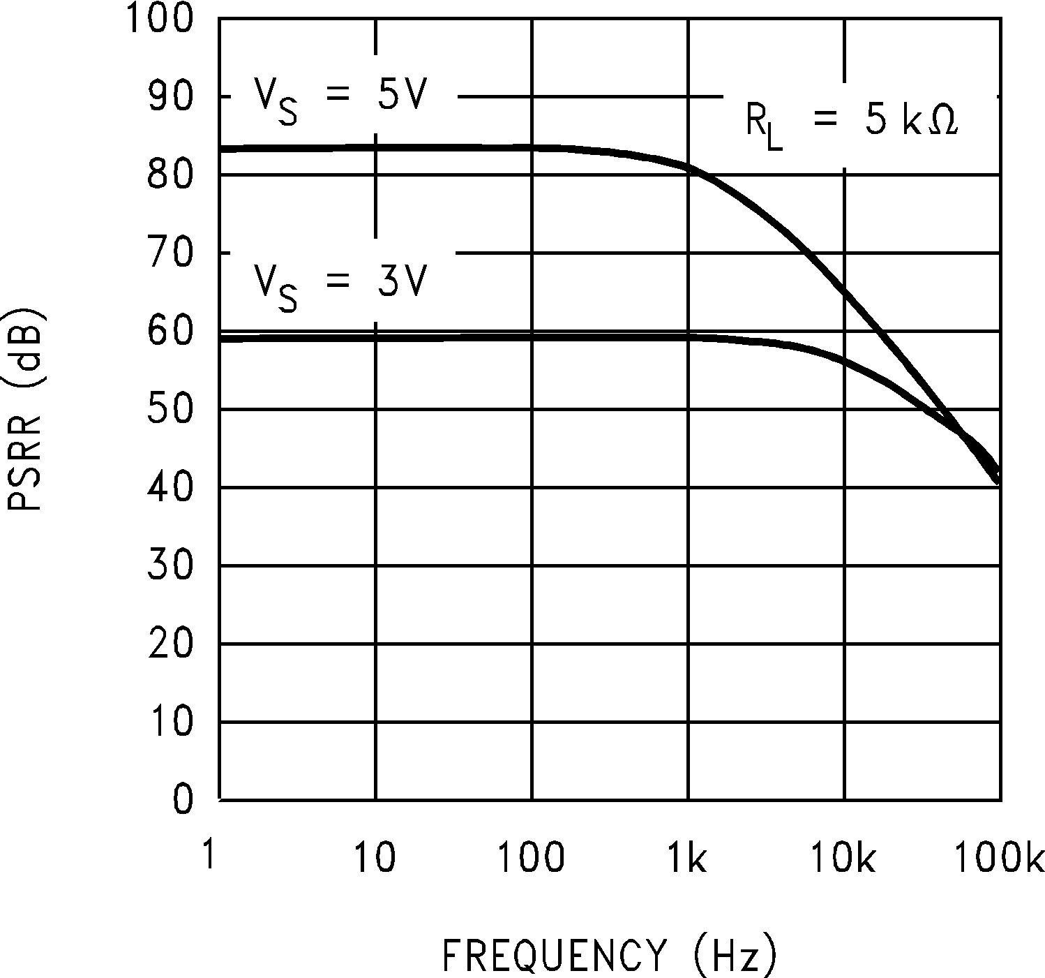 Figure 5-16 Positive PSRR vs Frequency
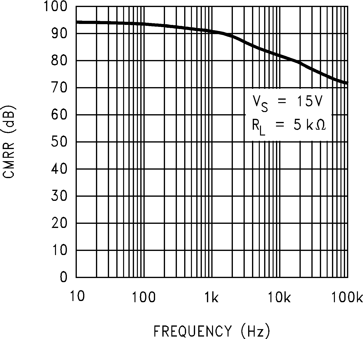 Figure 5-18 CMRR
vs Frequency
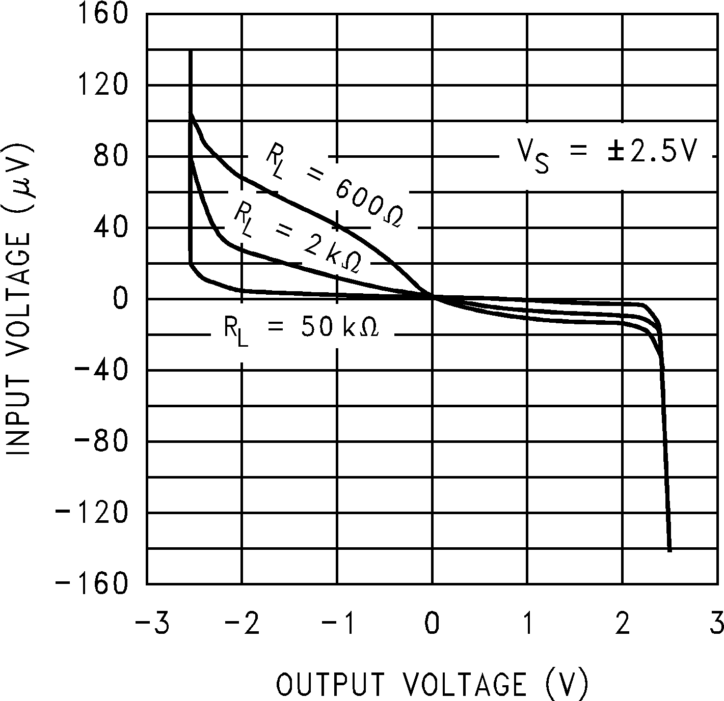 Figure 5-20 Input
Voltage vs Output Voltage
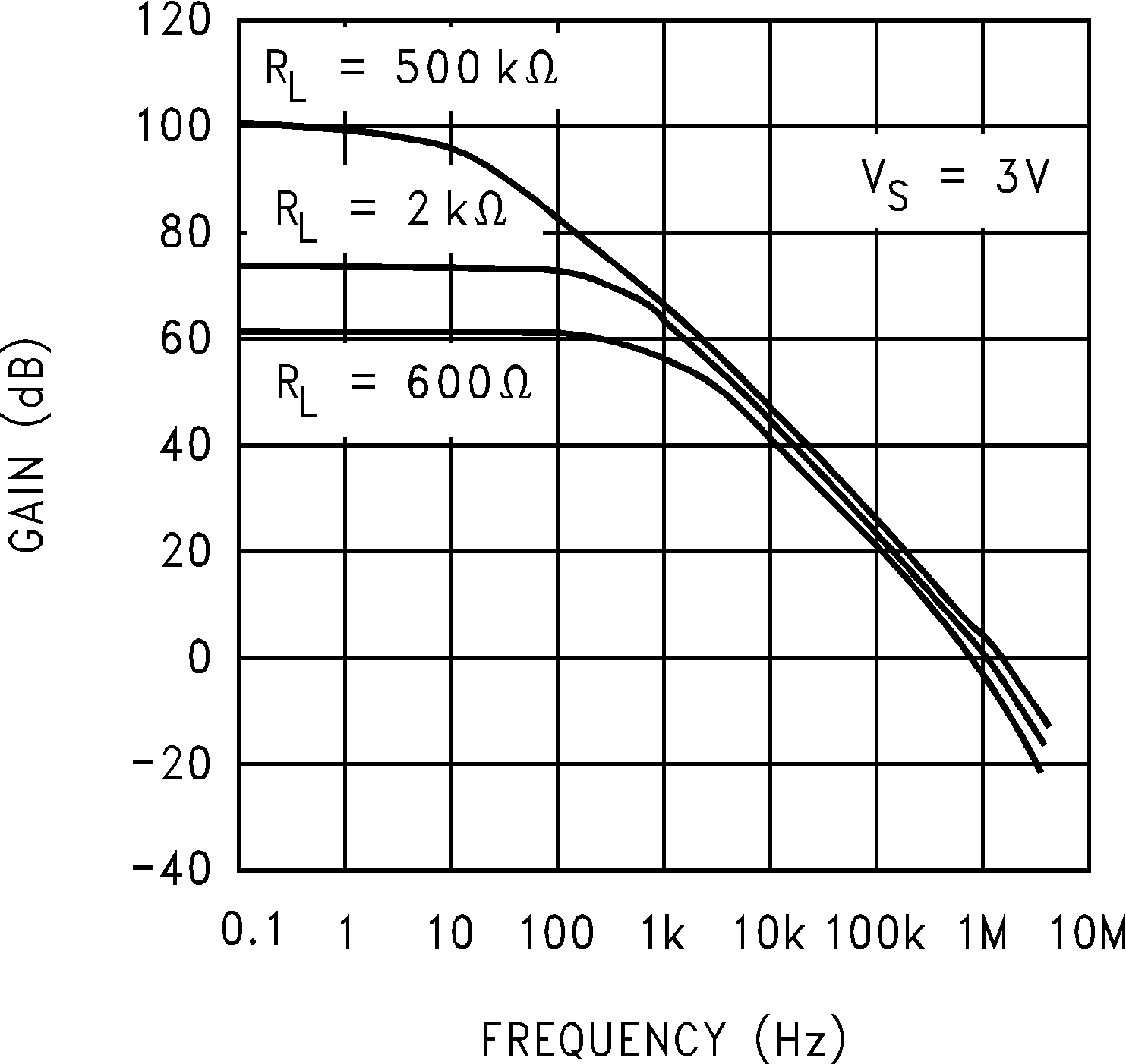 Figure 5-22 Open-Loop Frequency Response
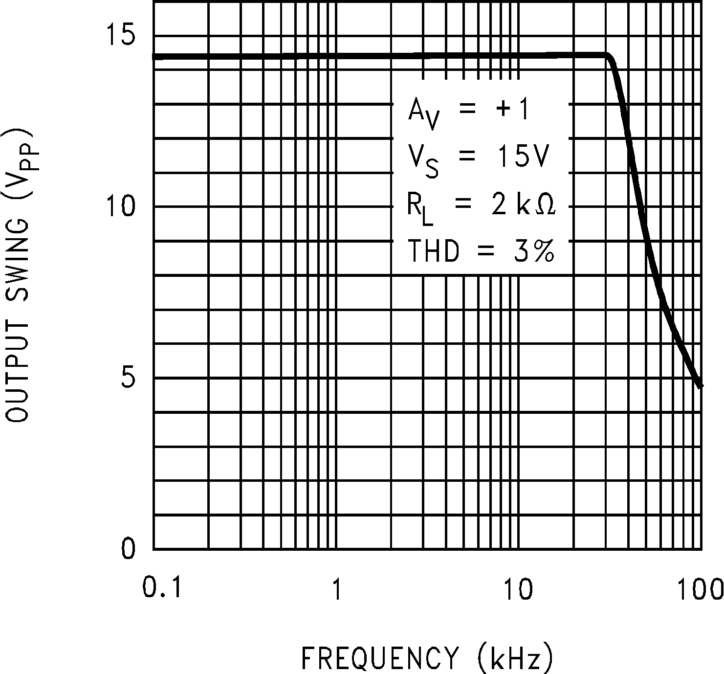 Figure 5-24 Maximum Output Swing vs Frequency
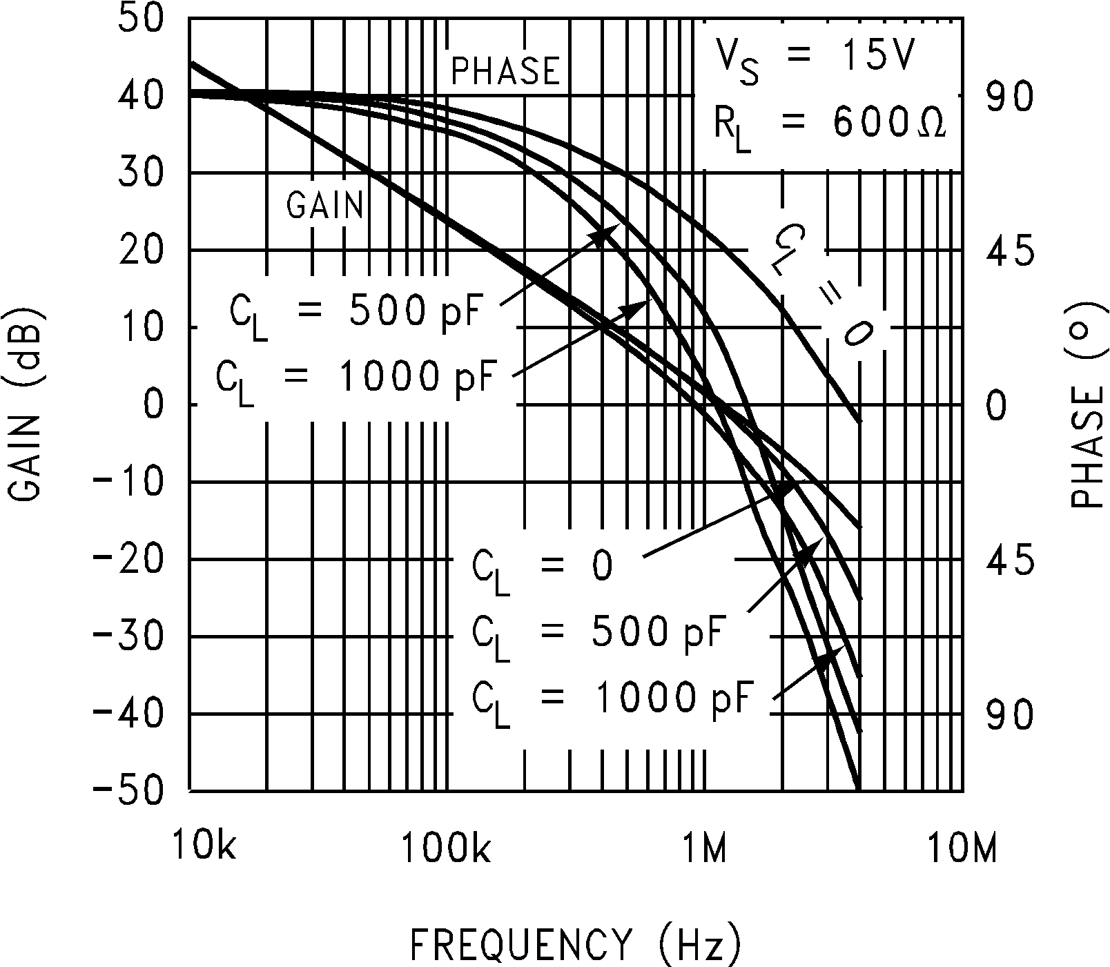 Figure 5-26 Gain
and Phase vs Capacitive Load
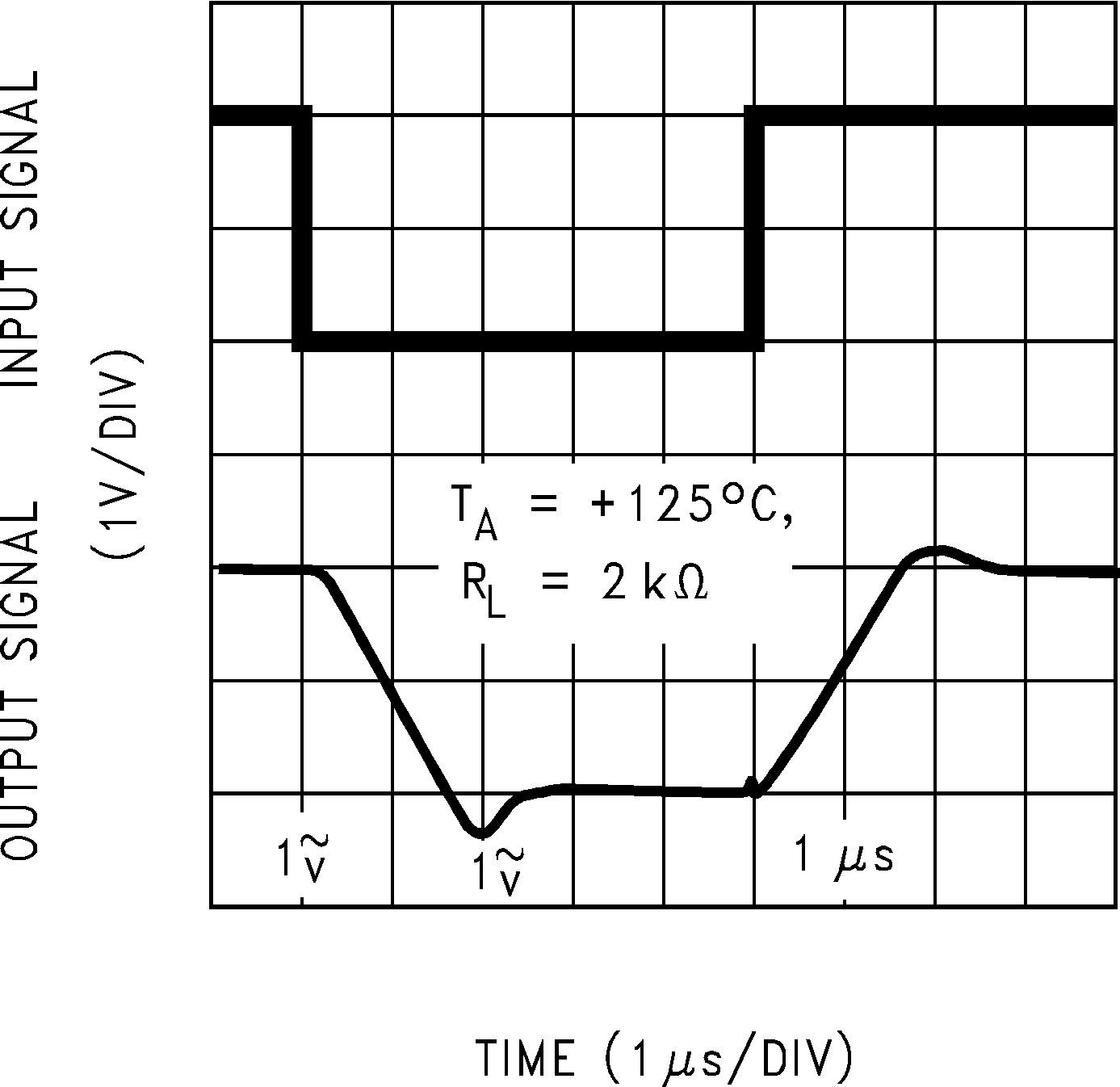 Figure 5-28 Noninverting Large Signal Pulse Response
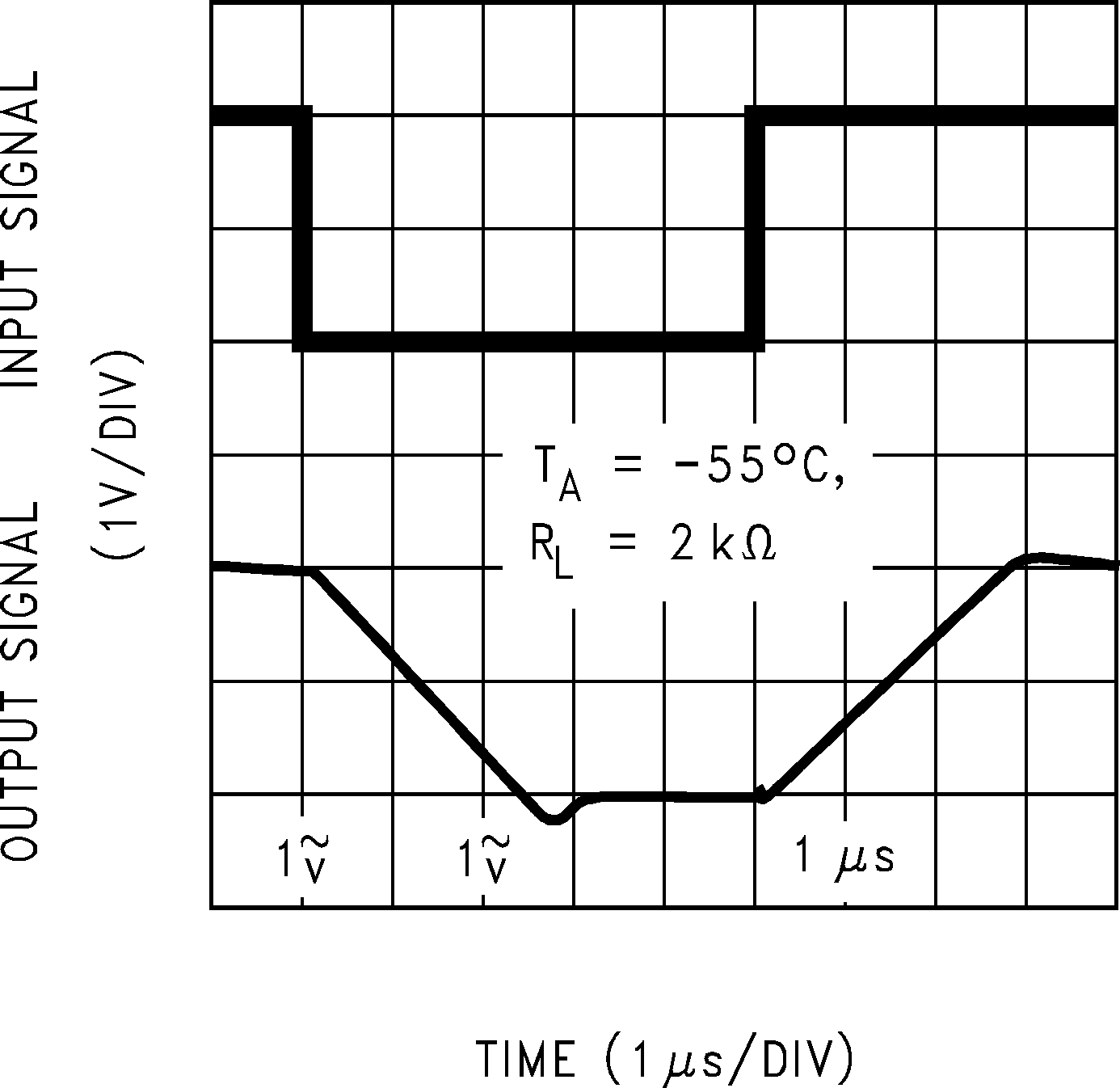 Figure 5-30 Noninverting Large Signal Pulse Response
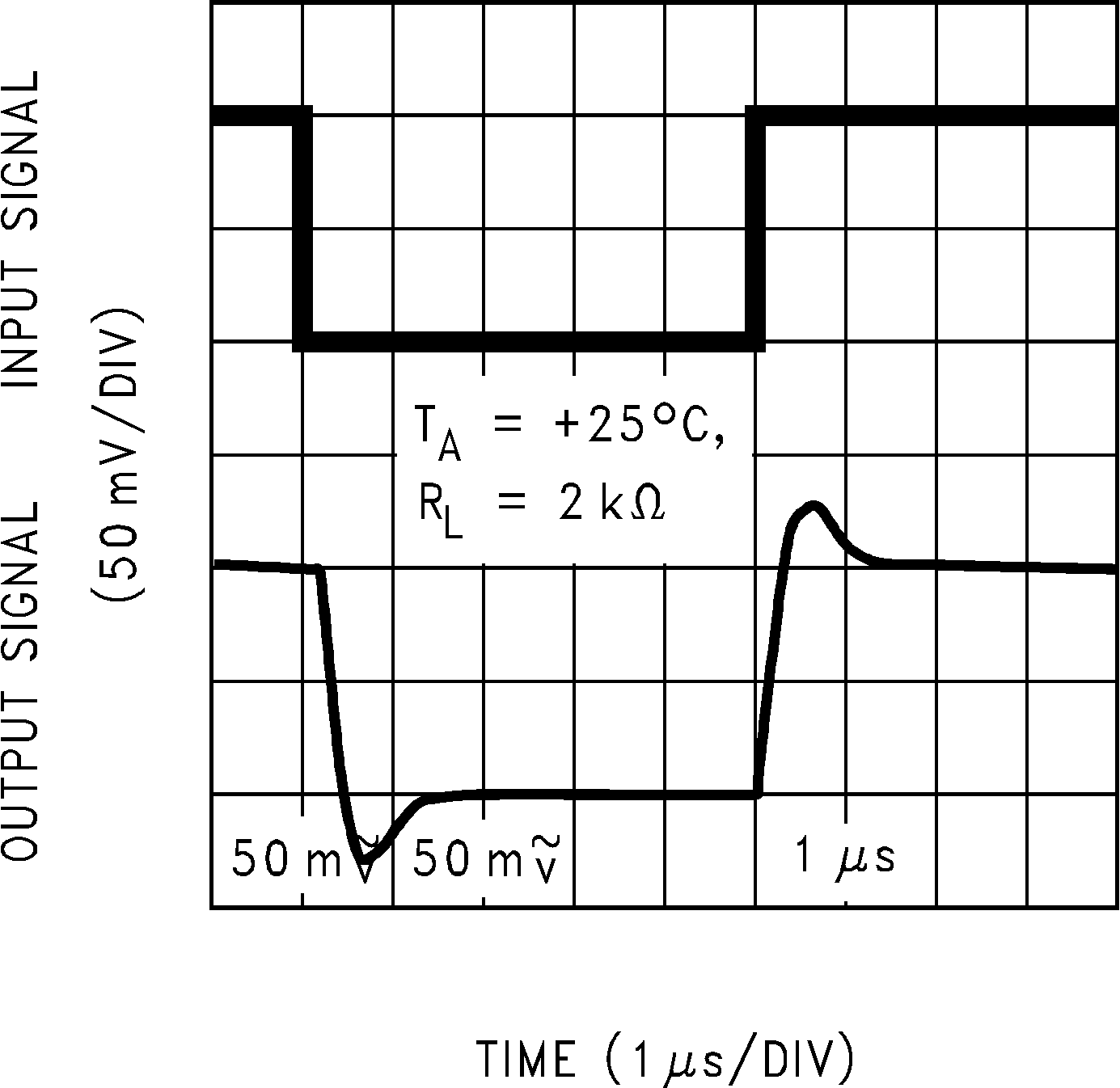 Figure 5-32 Noninverting Small Signal Pulse Response
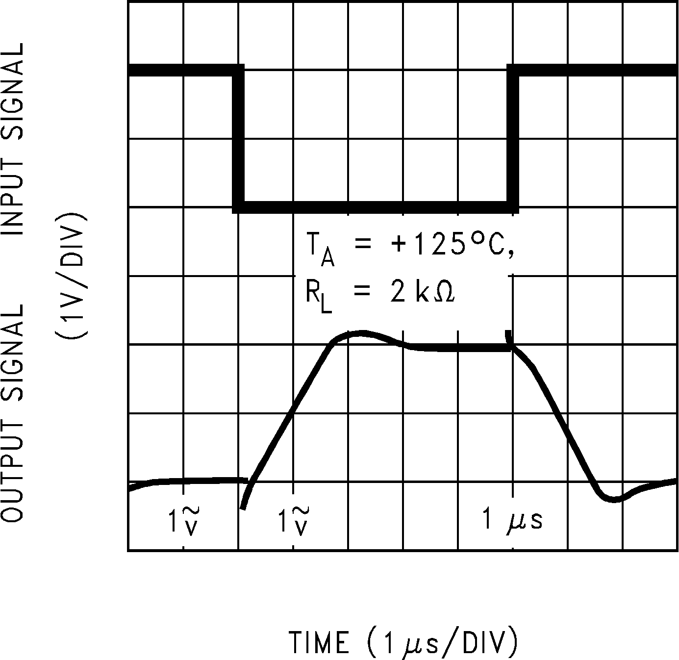 Figure 5-34 Inverting Large Signal Pulse Response
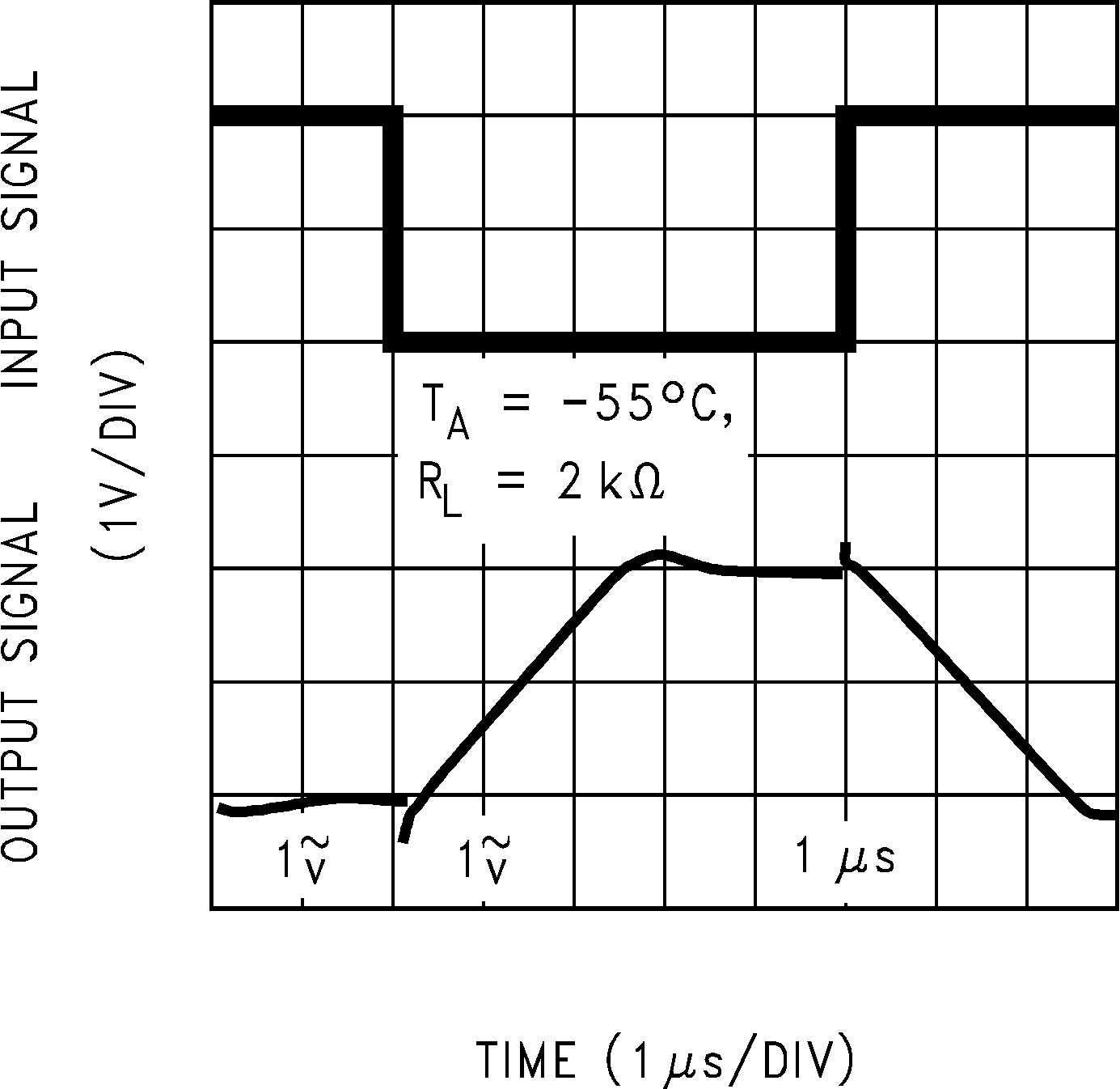 Figure 5-36 Inverting Large Signal Pulse Response
 Figure 5-38 Inverting Small Signal Pulse Response