SNOS674J October   1997  – September 2024 LMC6482 , LMC6484

PRODUCTION DATA  

  1.   1
  2. Features
  3. Applications
  4. Description
  5. Pin Configuration and Functions
  6. Specifications
    1. 5.1 Absolute Maximum Ratings
    2. 5.2 ESD Ratings
    3. 5.3 Recommended Operating Conditions
    4. 5.4 Thermal Information LMC6482
    5. 5.5 Thermal Information LMC6484
    6. 5.6 Electrical Characteristics: VS = 5V
    7. 5.7 Electrical Characteristics: VS = 3V
    8. 5.8 Typical Characteristics
  7. Detailed Description
    1. 6.1 Overview
    2. 6.2 Functional Block Diagram
    3. 6.3 Feature Description
      1. 6.3.1 Amplifier Topology
      2. 6.3.2 Input Common-Mode Voltage Range
      3. 6.3.3 Rail-to-Rail Output
    4. 6.4 Device Functional Modes
  8. Application and Implementation
    1. 7.1 Application Information
      1. 7.1.1 Upgrading Applications
      2. 7.1.2 Data Acquisition Systems
      3. 7.1.3 Instrumentation Circuits
    2. 7.2 Typical Applications
      1. 7.2.1 3V Single-Supply Buffer Circuit
        1. 7.2.1.1 Design Requirements
        2. 7.2.1.2 Detailed Design Procedure
          1. 7.2.1.2.1 Capacitive Load Compensation
          2. 7.2.1.2.2 Capacitive Load Tolerance
          3. 7.2.1.2.3 Compensating For Input Capacitance
          4. 7.2.1.2.4 Offset Voltage Adjustment
        3. 7.2.1.3 Application Curves
      2. 7.2.2 Typical Single-Supply Applications
    3. 7.3 Power Supply Recommendations
    4. 7.4 Layout
      1. 7.4.1 Layout Guidelines
      2. 7.4.2 Layout Example
  9. Device and Documentation Support
    1. 8.1 Device Support
      1. 8.1.1 Development Support
        1. 8.1.1.1 Spice Macromodel
        2. 8.1.1.2 PSpice® for TI
        3. 8.1.1.3 TINA-TI™ Simulation Software (Free Download)
        4. 8.1.1.4 DIP-Adapter-EVM
        5. 8.1.1.5 DIYAMP-EVM
        6. 8.1.1.6 TI Reference Designs
        7. 8.1.1.7 Analog Filter Designer
    2. 8.2 Receiving Notification of Documentation Updates
    3. 8.3 Support Resources
    4. 8.4 Trademarks
    5. 8.5 Electrostatic Discharge Caution
    6. 8.6 Glossary
  10. Revision History
  11. 10Mechanical, Packaging, and Orderable Information

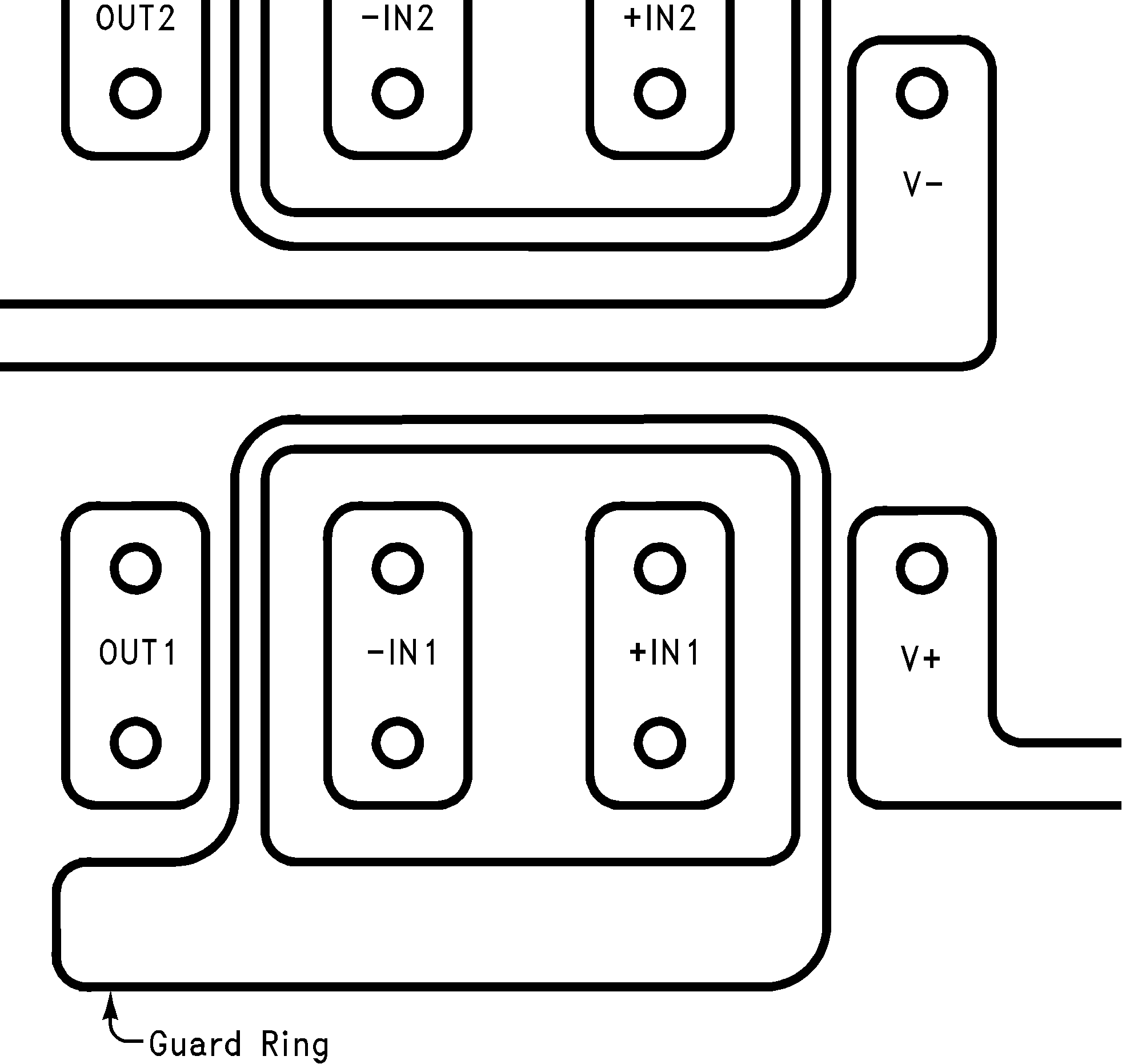
Layout Example

LMC6482  LMC6484 Example of Guard Ring in PCB Layout Typical Connections of Guard RingsFigure 7-26 Example of Guard Ring in PCB Layout Typical Connections of Guard Rings
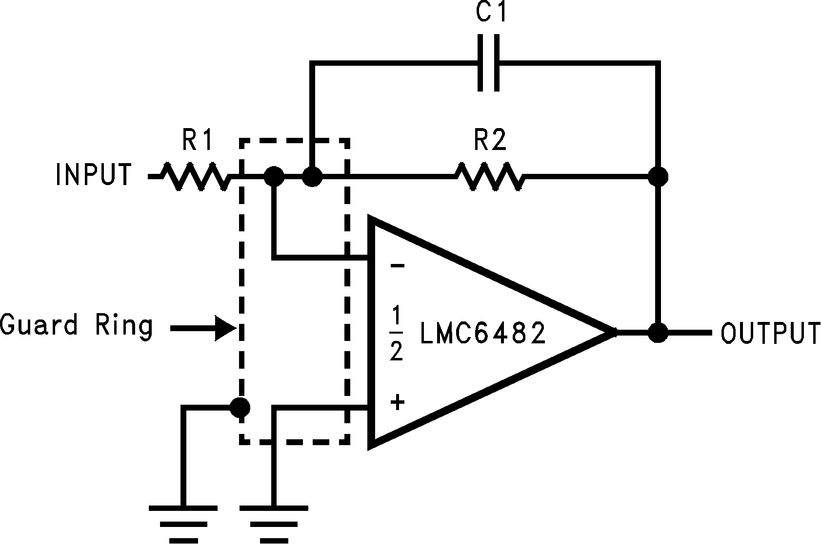
LMC6482  LMC6484 Inverting Amplifier Typical Connections of Guard RingsFigure 7-27 Inverting Amplifier Typical Connections of Guard Rings
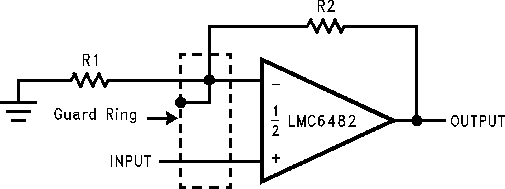
LMC6482  LMC6484 Noninverting Amplifier Typical Connections of Guard RingsFigure 7-28 Noninverting Amplifier Typical Connections of Guard Rings
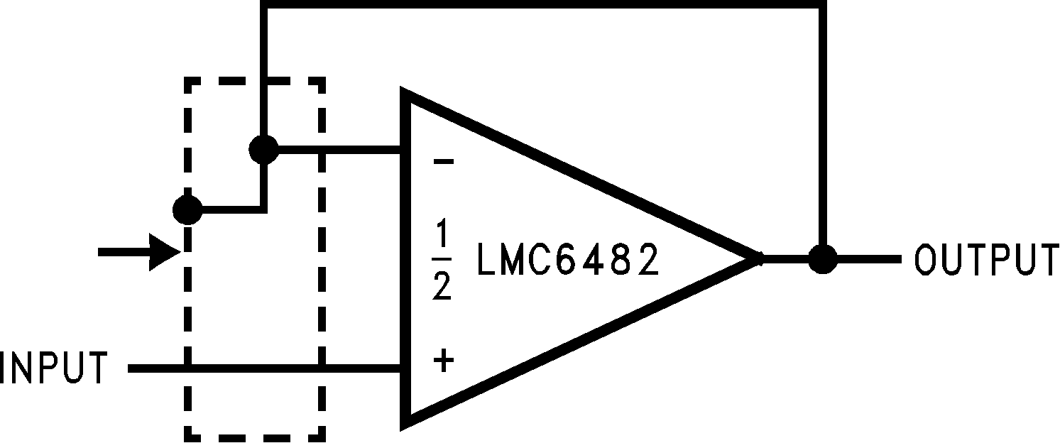
LMC6482  LMC6484 Follower Typical Connections of Guard RingsFigure 7-29 Follower Typical Connections of Guard Rings
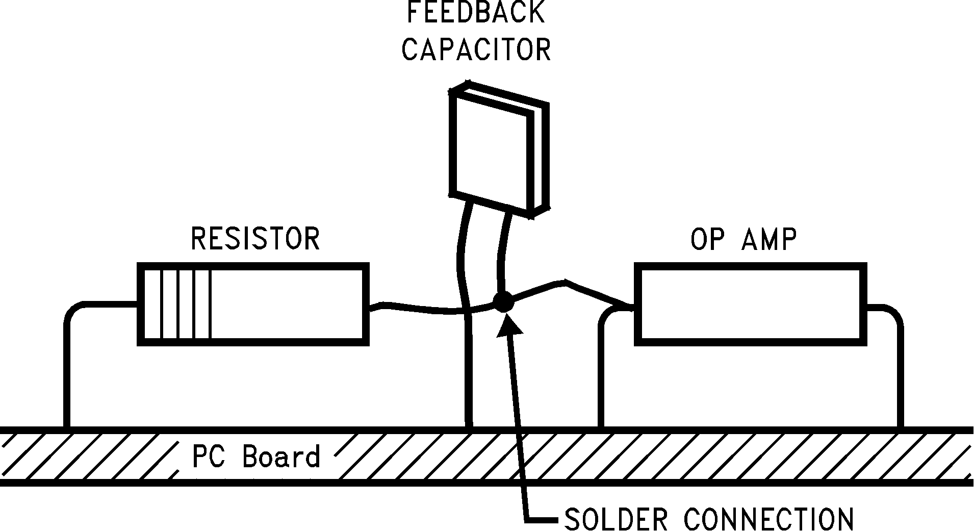
LMC6482  LMC6484 Air Wiring
Input pins are lifted out of PCB and soldered directly to components. All other pins connected to PCB.
Figure 7-30 Air Wiring