SNOS674J October   1997  – September 2024 LMC6482 , LMC6484

PRODUCTION DATA  

  1.   1
  2. Features
  3. Applications
  4. Description
  5. Pin Configuration and Functions
  6. Specifications
    1. 5.1 Absolute Maximum Ratings
    2. 5.2 ESD Ratings
    3. 5.3 Recommended Operating Conditions
    4. 5.4 Thermal Information LMC6482
    5. 5.5 Thermal Information LMC6484
    6. 5.6 Electrical Characteristics: VS = 5V
    7. 5.7 Electrical Characteristics: VS = 3V
    8. 5.8 Typical Characteristics
  7. Detailed Description
    1. 6.1 Overview
    2. 6.2 Functional Block Diagram
    3. 6.3 Feature Description
      1. 6.3.1 Amplifier Topology
      2. 6.3.2 Input Common-Mode Voltage Range
      3. 6.3.3 Rail-to-Rail Output
    4. 6.4 Device Functional Modes
  8. Application and Implementation
    1. 7.1 Application Information
      1. 7.1.1 Upgrading Applications
      2. 7.1.2 Data Acquisition Systems
      3. 7.1.3 Instrumentation Circuits
    2. 7.2 Typical Applications
      1. 7.2.1 3V Single-Supply Buffer Circuit
        1. 7.2.1.1 Design Requirements
        2. 7.2.1.2 Detailed Design Procedure
          1. 7.2.1.2.1 Capacitive Load Compensation
          2. 7.2.1.2.2 Capacitive Load Tolerance
          3. 7.2.1.2.3 Compensating For Input Capacitance
          4. 7.2.1.2.4 Offset Voltage Adjustment
        3. 7.2.1.3 Application Curves
      2. 7.2.2 Typical Single-Supply Applications
    3. 7.3 Power Supply Recommendations
    4. 7.4 Layout
      1. 7.4.1 Layout Guidelines
      2. 7.4.2 Layout Example
  9. Device and Documentation Support
    1. 8.1 Device Support
      1. 8.1.1 Development Support
        1. 8.1.1.1 Spice Macromodel
        2. 8.1.1.2 PSpice® for TI
        3. 8.1.1.3 TINA-TI™ Simulation Software (Free Download)
        4. 8.1.1.4 DIP-Adapter-EVM
        5. 8.1.1.5 DIYAMP-EVM
        6. 8.1.1.6 TI Reference Designs
        7. 8.1.1.7 Analog Filter Designer
    2. 8.2 Receiving Notification of Documentation Updates
    3. 8.3 Support Resources
    4. 8.4 Trademarks
    5. 8.5 Electrostatic Discharge Caution
    6. 8.6 Glossary
  10. Revision History
  11. 10Mechanical, Packaging, and Orderable Information

Description

The LMC6482 and LMC6484 (LMC648x) devices provide a common-mode range that extends to both supply rails. This rail-to-rail performance combined with excellent accuracy, due to a high CMRR, makes these devices unique among rail-to-rail input amplifiers. The devices are an excellent choice for systems that require a large input signal range, such as data acquisition. The LMC648x are also an excellent upgrade for circuits using limited common-mode range amplifiers, such as the TLC272, TLC274, TLC277 and TLC279.

Maximum dynamic signal range is provided in low voltage and single supply systems by the rail-to-rail output swing of the LMC648x. The rail-to-rail output swing is maintained for loads down to 600Ω of the device. Specified low-voltage characteristics and low-power dissipation make the LMC648x a great choice for battery-operated systems.

The LMC648x devices are available in PDIP, SOIC, and VSSOP packages.

Device Information
PART NUMBER CHANNEL COUNT PACKAGE(1)
LMC6482 Dual D (SOIC, 8)
DGK (VSSOP, 8)
P (PDIP, 8)
LMC6484 Quad D (SOIC, 14)
N (PDIP, 14)
For more information, see Section 10.
 
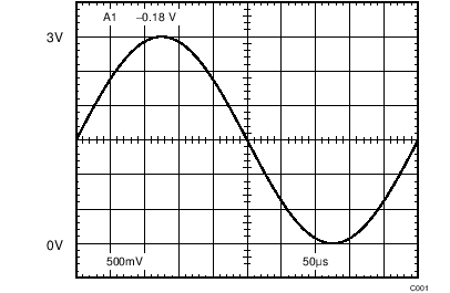
LMC6482  LMC6484 Rail-to-Rail Input
                            (VS = 3V)Rail-to-Rail Input (VS = 3V)
LMC6482  LMC6484 Unity-Gain Difference
                        AmplifierUnity-Gain Difference Amplifier