SNOSAQ2F July 2005 – August 2024 LMH6702QML-SP
PRODUCTION DATA
6.1.3 Capacitive Load Drive
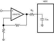
Figure 6-4 shows a typical application using the LMH6702 to drive an ADC.
 Figure 6-4 Input Amplifier to ADC
The series resistor, RS, between the amplifier output and the ADC input is critical to achieving best system performance. This load capacitance, if applied directly to the output pin, can quickly lead to unacceptable levels of ringing in the pulse response. The plot of RS and Settling Time vs CL in the Typical Characteristics is an excellent starting point for selecting RS. The value derived in that plot minimizes the step settling time into a fixed discrete capacitive load with the output driving a very light resistive load (1kΩ). Sensitivity to capacitive loading is greatly reduced after the output is loaded more heavily. Therefore, for cases where the output is heavily loaded, RS value can be reduced. The exact value can best be determined experimentally for these cases.
In applications where the LMH6702 is replacing the CLC409, take care when the device is lightly loaded and some capacitance is present at the output. As a result of the much higher frequency response of the LMH6702 compared to the CLC409, increased susceptibility to low value output capacitance (parasitic or inherent to the board layout or otherwise being part of the output load) is possible. As previously mentioned, this susceptibility is most noticeable when the LMH6702 resistive load is light. Parasitic capacitance can be minimized by careful layout. Addition of an output snubber R-C network also helps by increasing the high-frequency resistive loading.
Referring back to Figure 6-4, consider several additional constraints in driving the capacitive input of an ADC. There is an option to increase RS, band-limiting at the ADC input for either noise or Nyquist band-limiting purposes. However, increasing RS too much can induce an unacceptably large input glitch due to switching transients coupling through from the convert signal. Also, CIN is often a voltage-dependent capacitance. This input impedance nonlinearity induces distortion terms that increase as RS is increased. Therefore, attempt only slight adjustments up or down from the recommended RS value in optimizing system performance.