SNOSCZ4A April 2015 – October 2024 FDC1004-Q1
PRODUCTION DATA
- 1
- 1 Features
- 2 Applications
- 3 Description
- 4 Pin Configuration and Functions
- 5 Specifications
- 6 Detailed Description
- 7 Applications and Implementation
- 8 Device and Documentation Support
- 9 Revision History
- 10Mechanical, Packaging, and Orderable Information
4 Pin Configuration and Functions
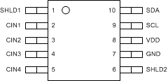
 Figure 4-1 DGS Package10 Pin VSSOPTop View
Table 4-1 Pin Functions
| PIN | TYPE(1) | DESCRIPTION | |
|---|---|---|---|
| NAME | NO. | ||
| SHLD1 | 1 | A | Capacitive Input Active AC Shielding. |
| CIN1 | 2 | A | Capacitive Input. The measured capacitance is connected between the CIN1 pin and GND. If not used, leave this pin as an open circuit. |
| CIN2 | 3 | A | Capacitive Input. The measured capacitance is connected between the CIN2 pin and GND. If not used, leave this pin as an open circuit. |
| CIN3 | 4 | A | Capacitive Input. The measured capacitance is connected between the CIN3 pin and GND. If not used, leave this pin as an open circuit. |
| CIN4 | 5 | A | Capacitive Input. The measured capacitance is connected between the CIN4 pin and GND. If not used, leave this pin as an open circuit. |
| SHLD2 | 6 | A | Capacitive Input Active AC Shielding. |
| GND | 7 | G | Ground |
| VDD | 8 | P | Power Supply Voltage. Decouple this pin to GND, using a low impedance capacitor, for example in combination with a 1μF tantalum and a 0.1μF multilayer ceramic. |
| SCL | 9 | I | Serial Interface Clock Input. Connects to the controller clock line. Requires pullup resistor if not already provided elsewhere in the system. |
| SDA | 10 | I/O | Serial Interface Bidirectional Data. Connects to the controller data line. Requires a pullup resistor if not provided elsewhere in the system. |
(1) P=Power, G=Ground, I=Input, O=Output, A=Analog,
I/O=Bidirectional Input/Output