SNOSDB6D December   2020  – October 2024 LMP7704-SP

PRODUCTION DATA  

  1.   1
  2. Features
  3. Applications
  4. Description
  5. Pin Configuration and Functions
  6. Specifications
    1. 5.1 Absolute Maximum Ratings
    2. 5.2 ESD Ratings
    3. 5.3 Recommended Operating Conditions
    4. 5.4 Thermal Information
    5. 5.5 Electrical Characteristics VS = 5 V
    6. 5.6 Electrical Characteristics VS = 10 V
    7. 5.7 Typical Characteristics
  7. Detailed Description
    1. 6.1 Overview
    2. 6.2 Functional Block Diagram
    3. 6.3 Feature Description
      1. 6.3.1 Radiation Hardened Performance
      2. 6.3.2 Engineering Model (Devices With /EM Suffix)
      3. 6.3.3 Diodes Between the Inputs
      4. 6.3.4 Capacitive Load
      5. 6.3.5 Input Capacitance
    4. 6.4 Device Functional Modes
      1. 6.4.1 Precision Current Source
  8. Application and Implementation
    1. 7.1 Application Information
      1. 7.1.1 Low Input Voltage Noise
      2. 7.1.2 Total Noise Contribution
    2. 7.2 Typical Application
      1. 7.2.1 Design Requirements
      2. 7.2.2 Detailed Design Procedure
      3. 7.2.3 Application Curves
    3. 7.3 Power Supply Recommendations
    4. 7.4 Layout
      1. 7.4.1 Layout Guidelines
      2. 7.4.2 Layout Example
  9. Device and Documentation Support
    1. 8.1 Related Documentation
    2. 8.2 Receiving Notification of Documentation Updates
    3. 8.3 Support Resources
    4. 8.4 Trademarks
    5. 8.5 Electrostatic Discharge Caution
    6. 8.6 Glossary
  10. Revision History
  11. 10Mechanical, Packaging, and Orderable Information

Capacitive Load

The LMP7704-SP can be connected as a noninverting unity gain follower. This configuration is the most sensitive to capacitive loading.

The combination of a capacitive load placed on the output of an amplifier along with the amplifier output impedance creates a phase lag, which in turn reduces the phase margin of the amplifier. If the phase margin is significantly reduced, the response is either underdamped or oscillated.

To drive heavier capacitive loads, use an isolation resistor, labeled as RISO in Figure 6-2. By using this isolation resistor, the capacitive load is isolated from the amplifier output, and thus, the pole caused by CL is no longer in the feedback loop. The larger the value of RISO, the more stable the output voltage. If values of RISO are sufficiently large, the feedback loop is stable, independent of the value of CL. However, larger values of RISO result in reduced output swing and reduced output current drive.
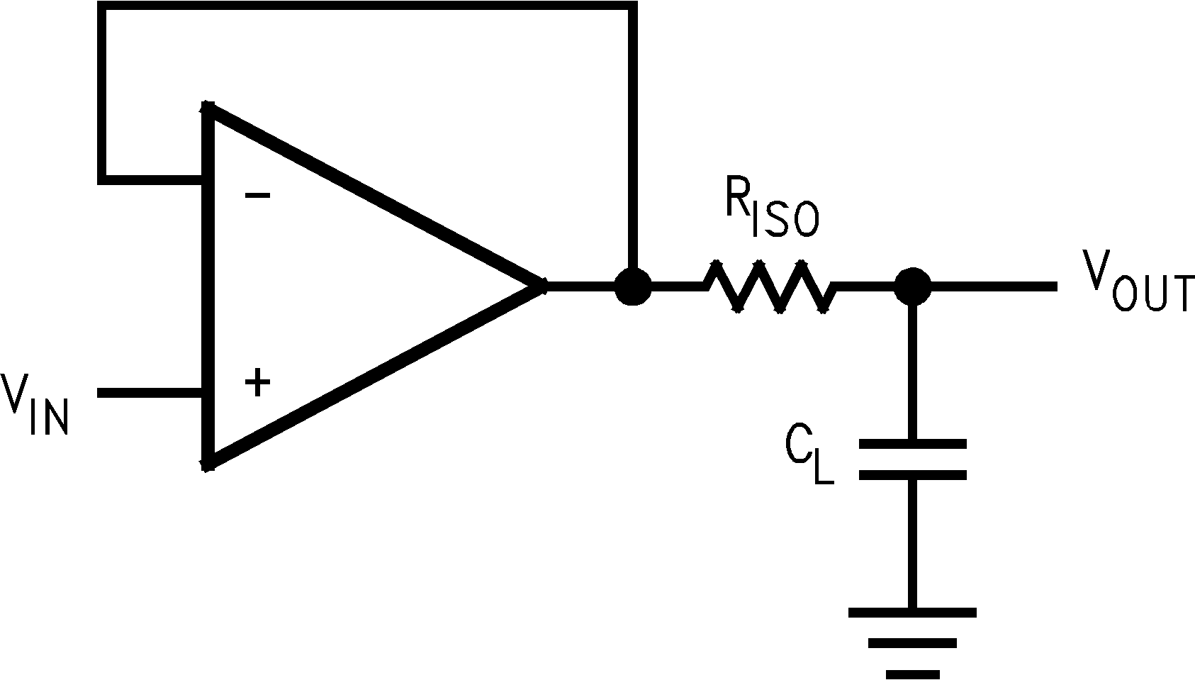
LMP7704-SP Isolating Capacitive LoadFigure 6-2 Isolating Capacitive Load