SNOSDB7 December 2020 LM74500-Q1
PRODUCTION DATA
- 1 Features
- 2 Applications
- 3 Description
- 4 Revision History
- 5 Pin Configuration and Functions
- 6 Specifications
- 7 Typical Characteristics
- 8 Detailed Description
-
9 Application and Implementation
- 9.1 Reverse Battery Protection for Automotive Body Control Module Applications
- 9.2 Reverse Polarity Protection
- 9.3 Application Information
- 10Power Supply Recommendations
- 11Layout
- 12Device and Documentation Support
- 13Mechanical, Packaging, and Orderable Information
7 Typical Characteristics
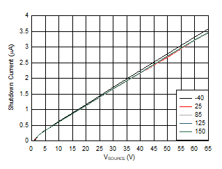 Figure 7-1 Shutdown Supply Current vs Supply Voltage
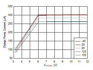 Figure 7-3 Charge Pump Current vs Supply Voltage at VCAP = 6 V
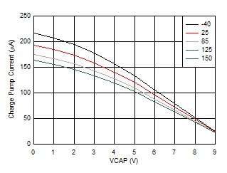 Figure 7-5 Charge Pump V-I Characteristics at VSOURCE = 3.2 V
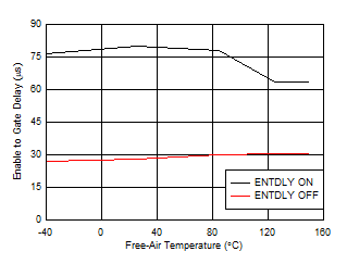 Figure 7-7 Enable to Gate Delay vs Temperature
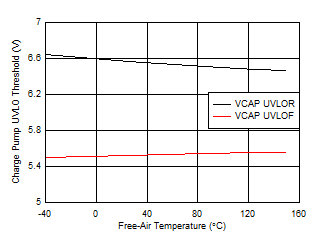 Figure 7-9 Charge Pump UVLO Threshold vs Temperature
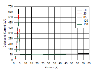 Figure 7-2 Operating Quiescent Current vs Supply Voltage
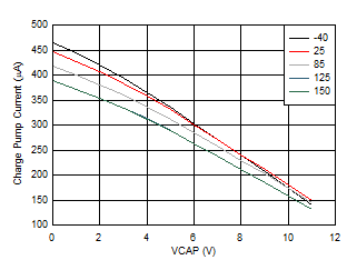 Figure 7-4 Charge Pump V-I Characteristics at VSOURCE > = 12 V
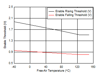 Figure 7-6 Enable Rising and Falling threshold vs Temperature
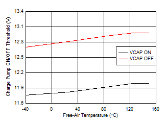 Figure 7-8 Charge Pump ON/OFF Threshold vs Temperature
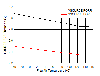 Figure 7-10 VSOURCE POR Threshold vs Temperature