SNOU170A August 2020 – December 2020
5 Quick Start Procedure
Note: DO NOT TURN ON POWER SUPPLY UNTIL ALL
CONNECTIONS TO THE DEVICE ARE MADE TO THE BOARD.
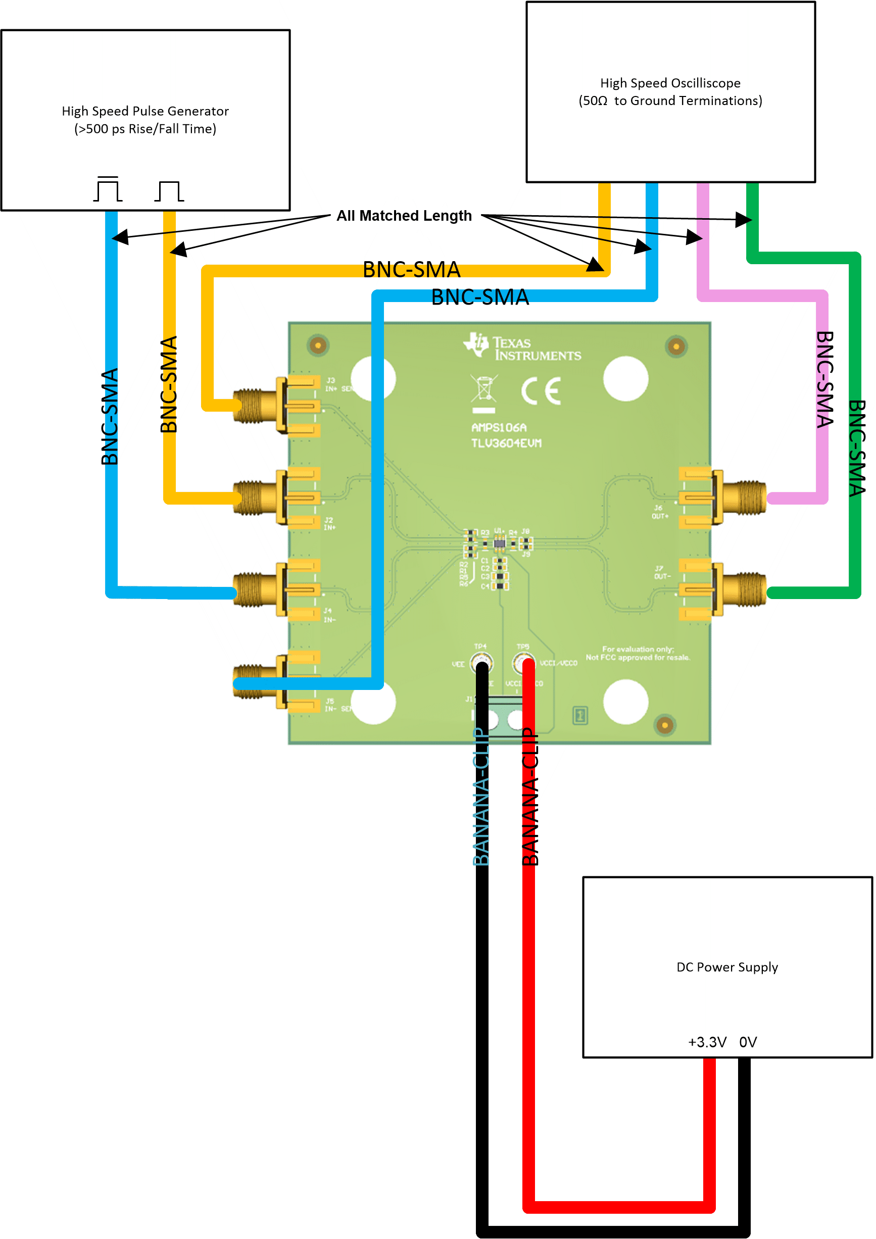
- Set VCCI/VCCO Power Supply to 3.3V and disable the power supply output
- Connect positive terminal supply to TP5, and negative terminal to TP4
- Ensure that cables connecting to IN+, IN-, IN+SENSE, IN-SENSE, OUT+, and OUT- are matched length and impedance. Perform any deskewing if necessary.
- Set the function generator to produce a square wave output with 100mVpp at 50MHz, with a DC offset of 1.65V. Disable the signal generator output. Connect the output to IN+.
- If available, use the second channel on the function generator to create a complementary signal to the one created in step 3. Disable the signal generator output. Connect the output to IN-.
- If a second channel or another function generator is not available, use a power supply set to 1.65V. Disable the output and connect to IN-. An adapter to connect the SMA connector on the board may be needed.
- Connect OUTP and OUTN to a 50Ω terminated scope. Alternatively, use a differential probe with a 100Ω termination and connect to the oscilloscope.
- Connect IN+SENSE and IN-SENSE to a 50Ω terminated scope channel.
- Enable the power supply and the signal generator.
- Verify the supply current is < 17.5mA
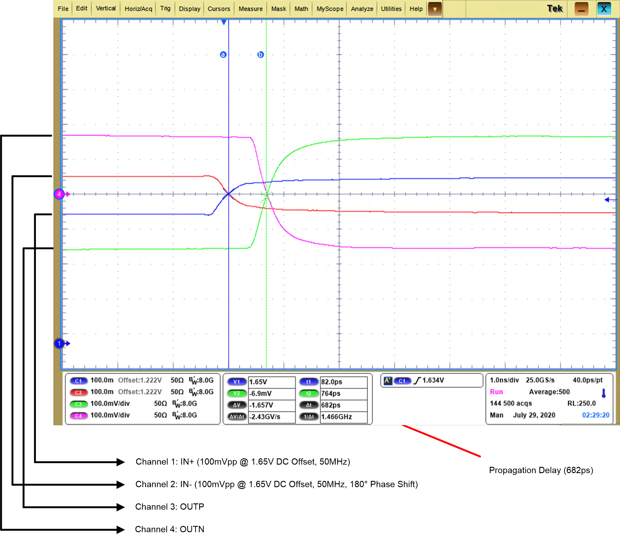
- Monitor and verify the inputs from IN+SENSE and IN-SENSE
- Monitor and verify the outputs for OUT+ and OUT-
 Figure 5-1 TLV3604 EVM Quick Start Setup
 Figure 5-2 Quick Start Example.