SNOU179A May 2021 – September 2021 LM74501-Q1
3.1.1 LM74501-Q1EVM Startup
- A startup pulse from 0 V to 12 V is applied at the input of the LM74501-Q1EVM.
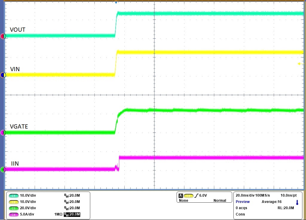
- Figure 3-1 shows the input voltage (CH2) rises from 0 V to 12 V and the gate voltage (CH3) comes up after input voltage crosses device PoR threshold.
- The gate of external N-FET is fully enhanced and FET is turned on. Output voltage (CH1) rises smoothly from 0 V to 12 V.
 Figure 3-1 LM74501-Q1EVM Startup