SNOU182 February 2021 TLV3605
6.3 Outputs
R10 is only needed if it is preferred to measure the LVDS output directly across the component, or if the board is being used to feed directly to the inputs of another interconnect device such as an FPGA. Otherwise it can be left uninstalled.
 Figure 6-3 Output Side
Schematic
Figure 6-3 Output Side
SchematicJ21 and J22 are installed with 0.1 uF capacitors. If probes are unavailable to measure the LVDS output across R10 or with a differential probe, these capacitors allow for the AC portion of the signal to be seen on a 50 Ω terminated scope. If equipment is available to measure the LVDS output with a respect to the 100 Ω resistor or with a differential probe, then J21 and J22 can be replaced with 0 Ω resistors to keep the DC integrity of the output signal.
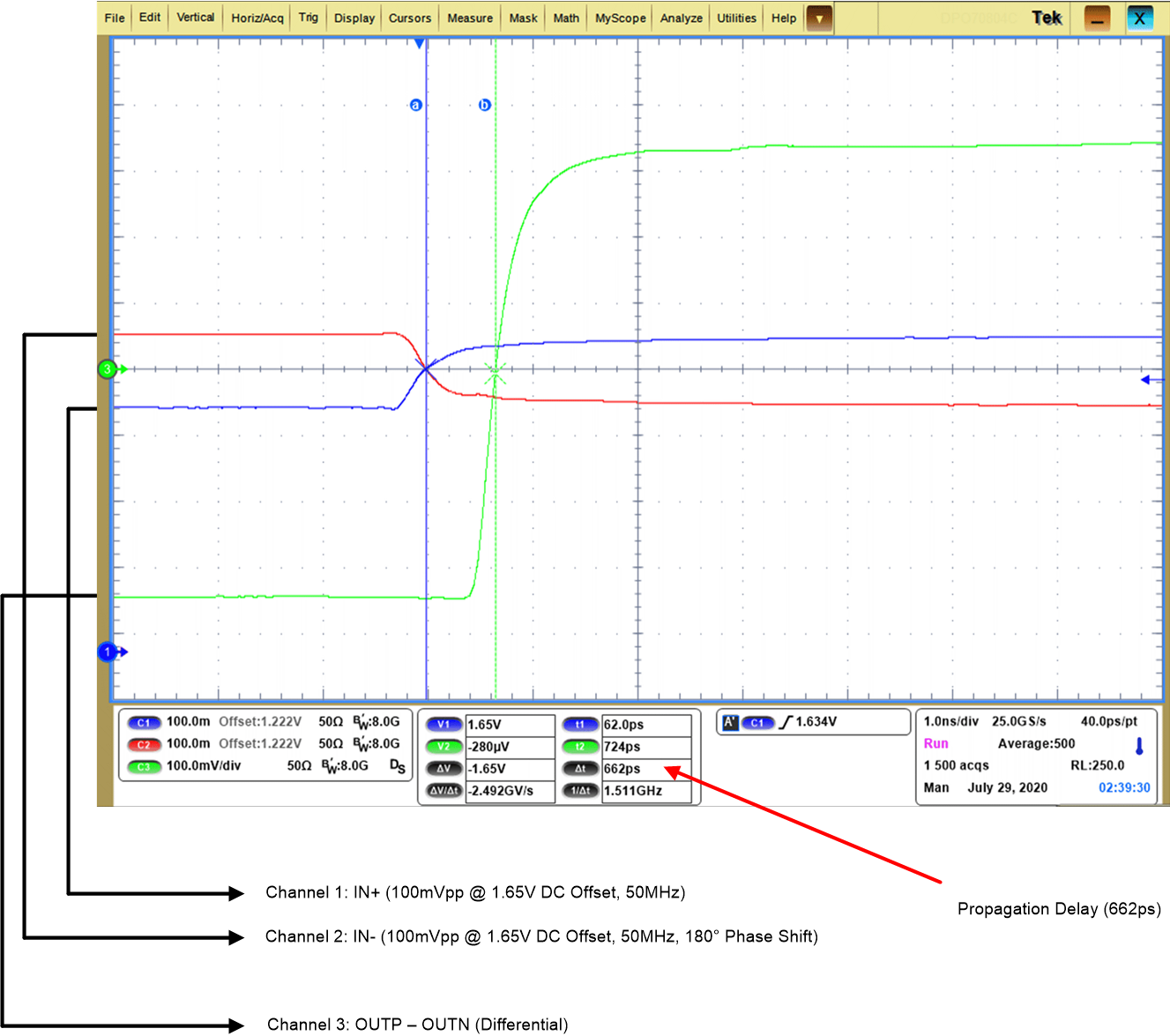
 Figure 6-4 Differential Output of TLV3605EVM