SNOU205 December 2024 LMG2650
2.1 LMG2650EVM-100 Daughtercard
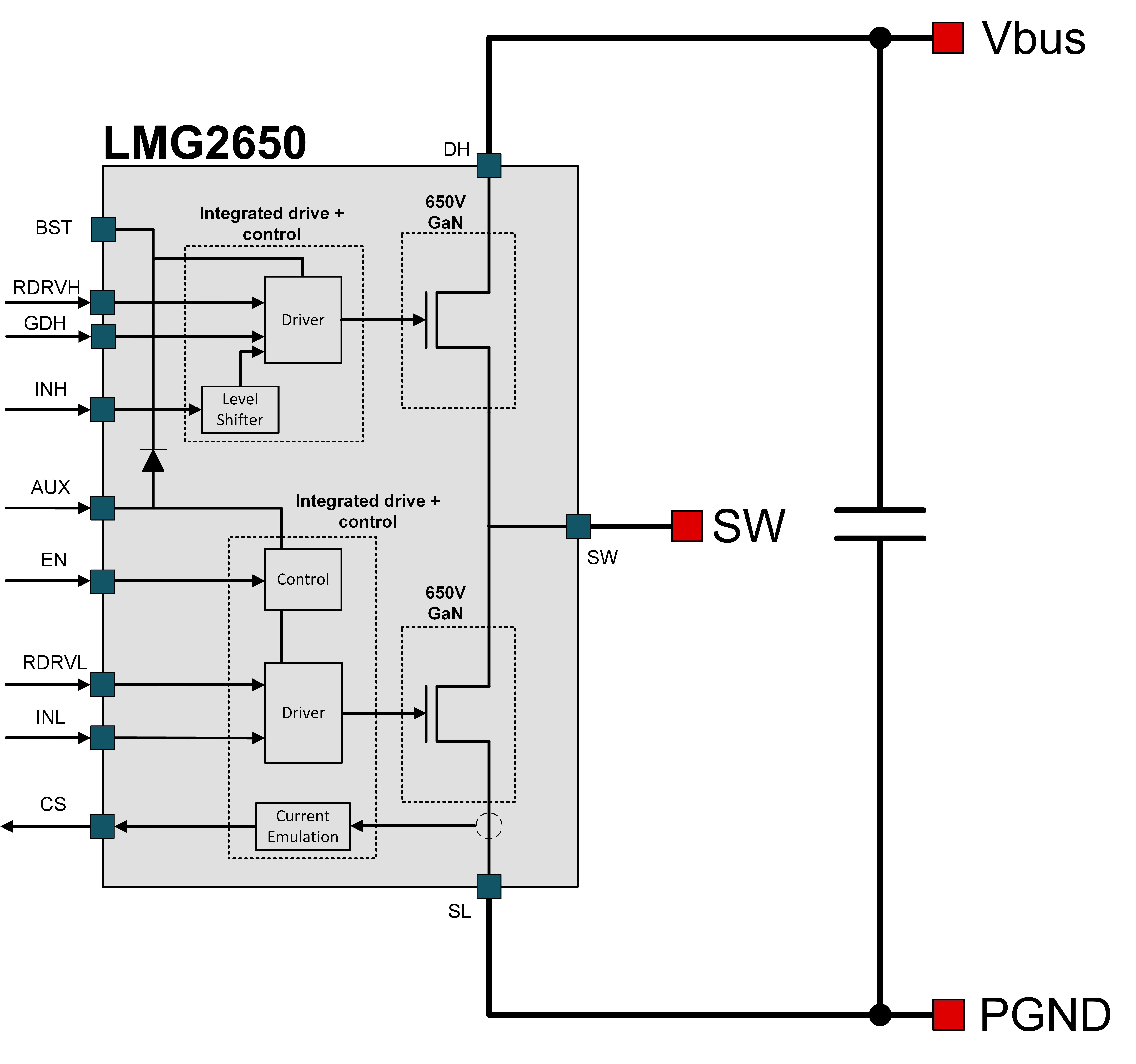
The LMG2650EVM-100 has one LMG2650 device with two GaN FETs in a half-bridge configuration. All the bias and level shifting components are included, which allows low-side referenced signals to control both FETs. High-frequency decoupling capacitors are included on the power stage in an optimized layout to minimize parasitic inductance and reduce voltage overshoot.
The layout of the board is critical to the performance and functionality of the device. TI recommends a four-layer or higher layer count board to reduce the parasitic inductance of the layout to the best performance. Layout guidelines are provided in the LMG2650 650V 95mΩ GaN Half Bridge with Integrated Driver and Current Sense Emulation data sheet to optimize the solder-joint reliability, power loop inductance, signal to ground connection, switched-node capacitance and thermal heat dissipation.
There is a 12 logic pin header on the LMG2650EVM-100 with 8 pins used for active logic and 4 with no connections
| PIN | PIN DESIGNATION | DESCRIPTION |
|---|---|---|
| LS PWM | 1 | Logic gate signal input for low-side LMG2650. Compatible with both 3.3V and 5V logic. Referenced to AGND. |
| HS PWM | 8 | Logic gate signal input for high-side LMG2650. Compatible with both 3.3V and 5V logic. Referenced to AGND. |
| 12V | 9 | Auxiliary power input for LMG2650EVM-100. |
| 5V | 3,6,10 | 5V auxiliary power for FAULT signal pull-up resistor and circuit debugging. |
| AGND | 11,12 | Logic and bias power ground return pin. Functionally isolated from PGND. |
There are six power pins on the LMG2650EVM-100.
| PIN | DESCRIPTION |
|---|---|
| SW | Switch node of the half-bridge configuration. |
| HV | Input DC voltage of the half-bridge configuration. |
| PGND | Power ground of the half-bridge configuration. Functionally isolated from AGND. |
High-voltage levels are present on the evaluation module whenever energized. Take proper precautions when working with the EVM.
 Figure 2-1 LMG2650EVM Block Diagram