SNOU209 December   2024


  1.   1
  2.   Description
  3.   Features
  4.   Applications
  5.   5
  6. 1Evaluation Module Overview
    1. 1.1 Introduction
    2. 1.2 Kit Contents
    3. 1.3 Specification
    4. 1.4 Device Information
    5. 1.5 General TI High Voltage Evaluation User Safety Guidelines
      1. 1.5.1 Safety and Precautions
  7. 2Hardware
    1. 2.1 LMG2656EVM-102 Daughtercard
      1. 2.1.1 Test Points
      2. 2.1.2 Integrated Current Sensing
      3. 2.1.3 Enable Pin
      4. 2.1.4 GDH
      5. 2.1.5 Power Pins
      6. 2.1.6 Heat Sink
    2. 2.2 Motherboard
      1. 2.2.1 Bias Supply
      2. 2.2.2 PWM Input
      3. 2.2.3 Fault Protection
    3. 2.3 Recommended Footprint
    4. 2.4 Test Equipment
    5. 2.5 Test Procedure When Paired With LMG342X-BB-EVM
      1. 2.5.1 Setup
      2. 2.5.2 Start-Up and Operating Procedure
      3. 2.5.3 Test Results
      4. 2.5.4 Shutdown Procedure
      5. 2.5.5 Additional Operating Notes
  8. 3Hardware Design Files
    1. 3.1 LMG2656EVM-102 Schematic
    2. 3.2 Motherboard Schematic
    3. 3.3 PCB Layout
    4. 3.4 Bill of Materials
  9. 4Additional Information
    1. 4.1 Trademarks
  10. 5Related Documentation

PCB Layout

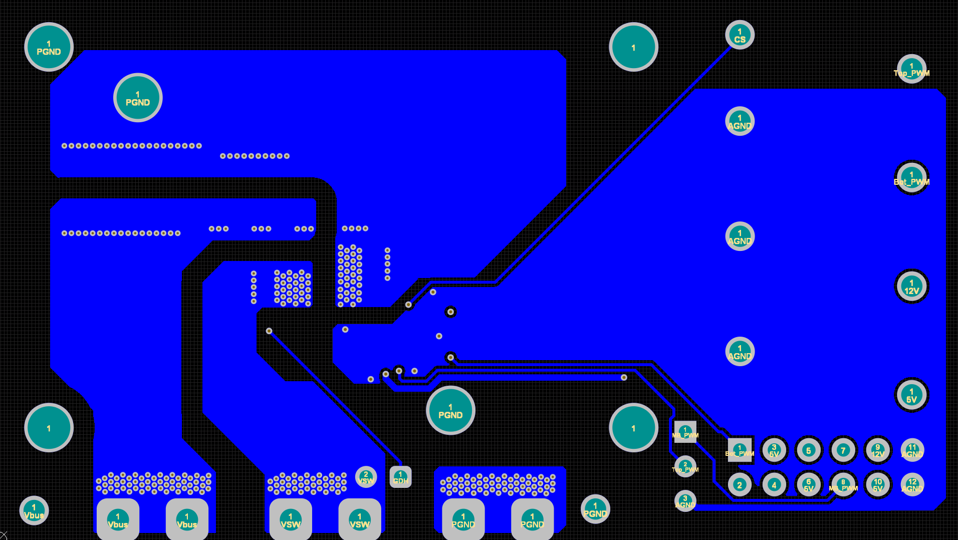
The PCB layers for this EVM are illustrated in Figure 3-3 through Figure 3-6.
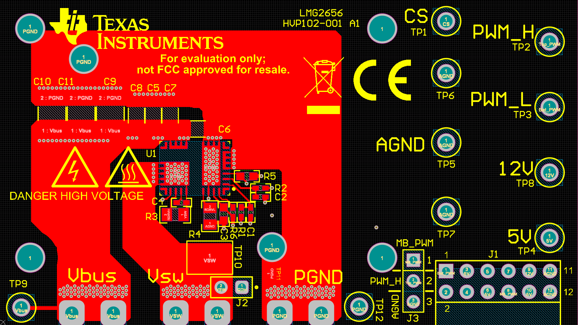
LMG2656EVM-102 Top Layer Figure 3-3 Top Layer
LMG2656EVM-102 Layer 2Figure 3-4 Layer 2
LMG2656EVM-102 Layer 3Figure 3-5 Layer 3
LMG2656EVM-102 Bottom LayerFigure 3-6 Bottom Layer