SNVA484B October 2011 – March 2024 LM5113
4 48V to 3.3V Conversion
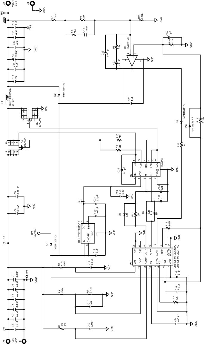
The LM5113 evaluation board can also be reconfigured for different switching frequency, dead time and output voltage. By adjusting the resistor R17, the PWM controller LM5025 can operate up to 1MHz. The dead time can be adjusted with the resistor R15, and/or with RCD circuitry at the inputs of the LM5113. The output voltage can be adjusted with R16 as follows:
Note that the maximum output power can be derated to verify the safe operation of the GaN FETs when the evaluation board is configured for the switching frequency beyond the preceding specifications.
Figure 5-1 shows the design for a 48V to 3.3V conversion. The switching frequency is set at 500kHz. Note that the bias supply for the control circuitry is generated from the internal LDO of the LM5025. To aid thermal dissipation, sufficient cooling must be provided for the LM5025. Alternatively, an external 10V supply can be connected to the terminal TP1 EXT VCC to provide the bias voltage for the control circuitry.
 Figure 4-1 Application Circuit: Input
48V, Output 3.3V, 10A, 500kHz