SNVA866A February 2019 – January 2023 LM5155 , LM5155-Q1 , LM51551 , LM51551-Q1
- How to design an Isolated Flyback using LM5155
- Trademarks
- 1Introduction
- 2Example Application
- 3Calculations and Component Selection
- 4Component Selection Summary
- 5Small Signal Frequency Analysis
- 6Revision History
3.2.1 Maximum Duty Cycle and Turns Ratio Selection
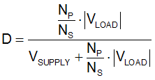
In CCM operation the duty cycle of the low side switch is calculated using Equation 2.

where
- NP is the number of turns on the primary side winding and assumed to be 1
- NS is the number of turns on the secondary side winding.
The maximum duty cycle occurs when the supply voltage is at the minimum value. By selecting the maximum duty cycle, the number of turns on the secondary winding is calculated. Selecting the duty cycle to be less than 50% brings two main benefits. First, it reduces the need for slope compensation which is required for stable operation when the duty cycle is greater than 50% in CCM operation. For some wide input voltage designs limiting the duty cycle below 50% might not be possible. The LM5155 provides programmable slope compensation for such designs. Second, the right-half plane zero of the modulator is pushed to high frequencies, helping to improve the load transient response and simplifying the control loop compensation calculations. For this design the maximum duty cycle (DMAX) is selected to be 40%. The number of turns on the secondary winding is calculated using Equation 3

NS is selected to be 0.5 turns. Selecting NS to be 0.5 turns the turns ratio to achieved in the fewest number of full turns. In this example the minimum number of turns is 2 on the primary winding and 1 turn on the secondary winding. With NS selected, Equation 4 is used to calculate the maximum duty cycle.

DMAX is calculated to be approximately 35.7%, below the target maximum duty cycle of 40%. The number of turns on the auxiliary winding is calculated using Equation 5

where
- VAUX is the auxiliary winding voltage