SNVA935A June 2020 – July 2021 LM60430 , LM60430-Q1 , LM60440 , LM60440-Q1
4.2 Enhanced HotRod QFN Thermal Performance
The LM60440 device is the industry’s smallest 4-A, 36-V converter with a package size of 3 mm × 2 mm. The package size is enabled by QFN package technology and the implementation of a PowerPad. The PowerPad is a ground connection in the middle of the IC used to improve thermal dissipation (Figure 2-7).
The symmetric QFN pin-out eases the layout – particularly to enable optimized thermal design. Figure 4-1 illustrates the LM60440AQEVM layout. The blue outline represents the placement of the LM60440 IC. Three thermal vias are placed under the IC from the PowerPad to the ground plane. The PowerPad is then connected to the larger ground plane through the AGND pin (pin 6). In addition the top corner ground pins are also used to remove heat from the IC.
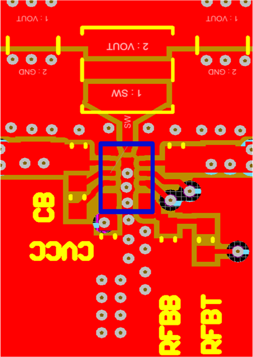 Figure 4-1 LM60440AQEVM Layout
Figure 4-2 illustrates the thermal image of the LM60440AQEVM. At a 12-V input, 5-V output, 4-A load, the IC temperature raises approximately 60⁰C. The maximum operating junction temperature of the LM60440 and LM60430 devices is 150⁰C. At the operating conditions of VIN = 12 V, VOUT = 5 V, and IOUT = 4 A, the efficiency of the LM60440 device at 87⁰C will be 89% (Figure 4-3).
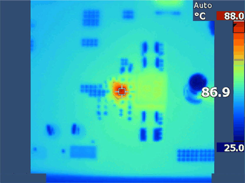 Figure 4-2 LM60440AQEVM Thermal Image (VIN = 12 V, VOUT = 5 V, IOUT = 4 A)
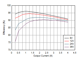 Figure 4-3 LM60440 Efficiency
vs Output Current (VIN = 12 V, VOUT = 5 V, IOUT = 4 A)
Figure 4-3 LM60440 Efficiency
vs Output Current (VIN = 12 V, VOUT = 5 V, IOUT = 4 A)The total power dissipation is 2.2 W. The inductor used is the XAL6060-682MEB which has a DCR of 20.8 mΩ. To accurately calculate the temperature characteristic of the IC, the power dissipation of the IC alone must be calculated as Equation 1 and Equation 2 show.
The IC losses are 1.87 W. Then the characteristic θJA of the PCB can be calculated as Equation 3 shows.
Both the LMR33630 and LM60440 device are in a 3-mm × 2-mm package. For comparison, a similar procedure was completed for the LMR33630 device, and Figure 4-4 shows the thermal image.
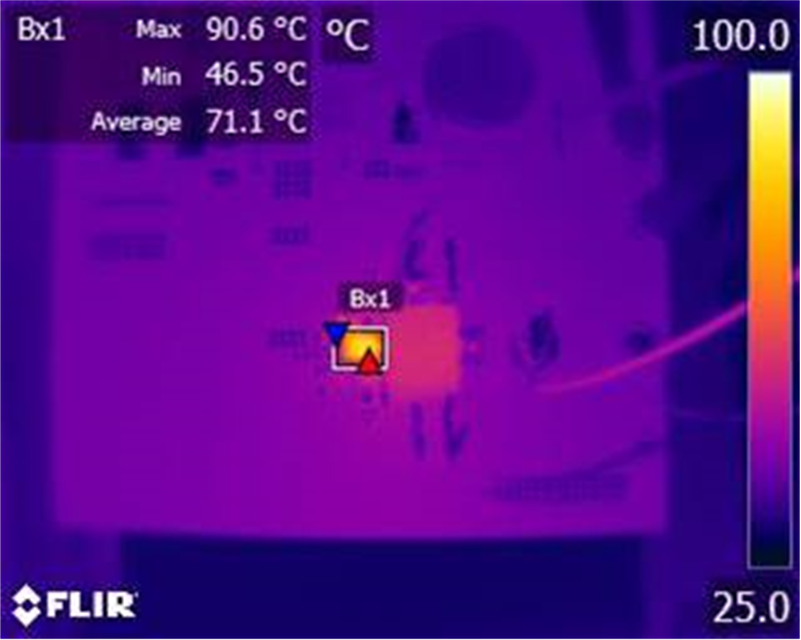 Figure 4-4 LMR33630 Thermal Image
The LMR33630 θJA was found to be 38.6⁰C/W. The Enhanced HotRod QFN package offers approximately a 13% improvement in thermal characteristics compared to the FCOL package technology. Figure 4-5 shows the LM60440 and LM60430 maximum load current versus ambient temperature curve. The LM60440 device is capable of operating at full load current at 85 ⁰C and the LM60430 device is capable of operating at full load current at 100⁰C.
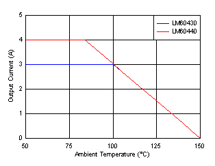 Figure 4-5 Maximum Current vs Ambient Temperature