SNVA935A June 2020 – July 2021 LM60430 , LM60430-Q1 , LM60440 , LM60440-Q1
2.2 Enhanced HotRod QFN Package
As discussed in Section 1, the Enhanced HotRod QFN package has evolved from the standard QFN package and the FCOL package. Before delving into the latest package technology, it is important to understand the merits of the construction of each of its parent packages.
A standard QFN package has wire-bonds connecting the silicon to the lead frame (Figure 2-1). These wire-bonds can have inductance in order of 2 nH, and during a switching event, its commutating current can be in the order of 2 A/ns which can result in voltage overshoot up to 4–5 V on switch-node. Furthermore, device package wire bonds contribute significantly to the parasitic inductance of the power loop where fast switching (current and voltage) edges—and possible leading-edge ringing related to body diode reverse recovery and MOSFET COSS charging—is rich in harmonic content. The corresponding switch node ringing poses a severe threat of H-field and E-field coupling and consequently increases conducted and radiated emissions (Figure 2-2).
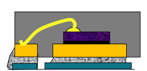 Figure 2-1 Standard QFN Package Diagram
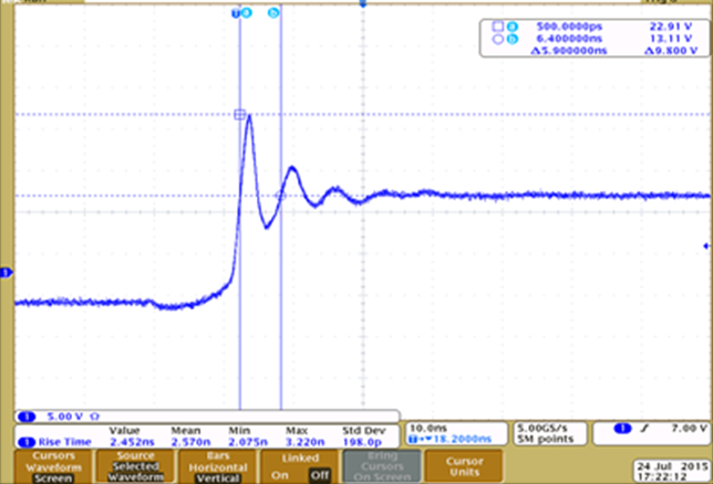 Figure 2-2 Switch Node Waveform (Standard QFN Package)
The LMR33630 utilized FCOL package technology, as shown in Figure 2-3, to eliminate the wire bonds by flipping the die on the lead frame to achieve the best possible EMI performance. The switch node waveform is shown in Figure 2-4 and the ringing has been eliminated. The trade-off of this technology is that the heat needs to dissipate through all the pins of the package. Due to the physical size limitation of each pin and absence of dedicated ground DAP for heat dissipation, the thermal performance of the FCOL package is limited compared to the standard QFN package. This observation is discussed in more detail in Section 4.
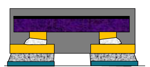 Figure 2-3 FCOL Package Diagram
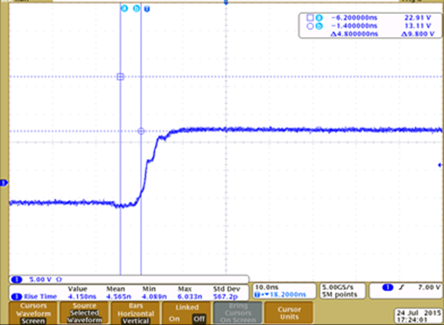 Figure 2-4 Switch Node Waveform (FCOL Package)
TI’s latest Enhanced HotRod QFN package offers next-generation technology to provide a low-EMI, high-power density solution in a standard QFN pinout for design familiarity and flexibility. The LM60440 and LM60440-Q1 devices are wide-VIN synchronous buck converters designed for low noise and EMI. The LM60440 device has an input voltage range of 3.8 V to 36 V capable of up to 4 A of load current. The LM60440 device has the same FCOL technology to eliminate the wire bond (expect same EMI performance), but utilizes a PowerPad (pin 13) consistent with a standard QFN package for better thermal relief and performance. In conclusion, Enhanced HotRod QFN package technology offers the best possible EMI performance and best possible thermal performance (as detailed in Section 4). In the following section, the Enhanced HotRod QFN Pin-Out (Figure 2-5) is examined in more detail.
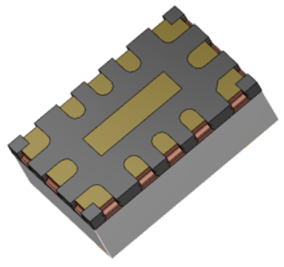 Figure 2-5 LM60440 Package
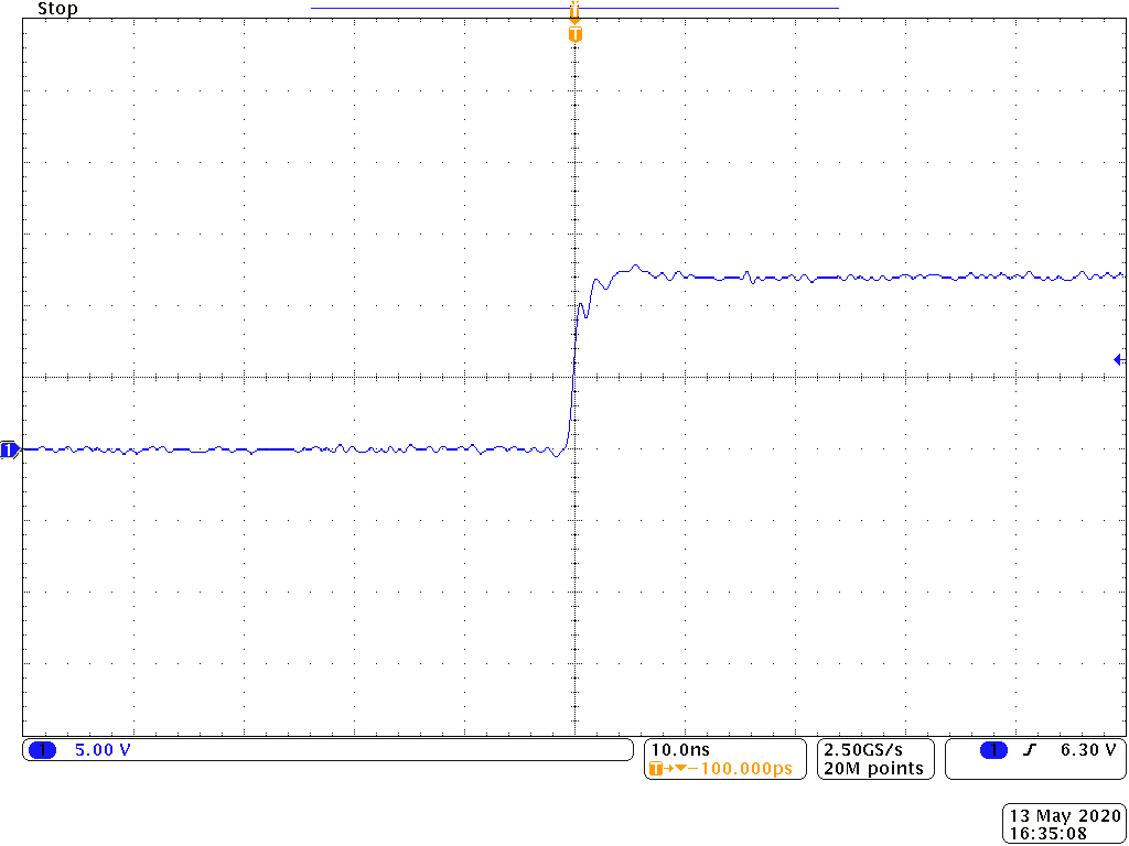 Figure 2-6 LM60440 Switch Node