SNVA941A June 2020 – November 2022 LM5156 , LM5156-Q1 , LM51561 , LM51561-Q1 , LM51561H , LM51561H-Q1 , LM5156H , LM5156H-Q1
- How to Design a Boost Converter Using the LM5156
- 1LM5156 Design Example
- 2Example Application
-
3Calculations and Component Selection
- 3.1 Switching Frequency
- 3.2 Inductor Calculation
- 3.3 Current Sense Resistor Calculation
- 3.4 Inductor Selection
- 3.5 Diode Selection
- 3.6 MOSFET Selection
- 3.7 Output Capacitor Selection
- 3.8 Input Capacitor Selection
- 3.9 UVLO Resistor Selection
- 3.10 Soft-Start Capacitor Selection.
- 3.11 Feedback Resistor Selection
- 3.12 Control Loop Compensation
- 3.13 Efficiency Estimation
- 4Component Selection Summary
- 5Small-Signal Frequency Analysis
- 6Revision History
3.12 Control Loop Compensation
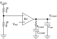
There are many different strategies to set the crossover frequency of the control loop, and placing the pole and zero of the error amplifier. In this section a general technique is described to adequately stabilize the control loop for a peak current mode controlled boost regulator in continuos conduction mode operation. A type II compensation network is implemented as shown in Figure 3-2. Type II compensation provides a programable low frequency zero and programable high frequency pole. For a detailed model of the control loop see Section 5. The loop compensation selection process is broken down into a number of distinct steps described in the following sections.
 Figure 3-2 Type II Compensation
Network