SNVA941A June 2020 – November 2022 LM5156 , LM5156-Q1 , LM51561 , LM51561-Q1 , LM51561H , LM51561H-Q1 , LM5156H , LM5156H-Q1
- How to Design a Boost Converter Using the LM5156
- 1LM5156 Design Example
- 2Example Application
-
3Calculations and Component Selection
- 3.1 Switching Frequency
- 3.2 Inductor Calculation
- 3.3 Current Sense Resistor Calculation
- 3.4 Inductor Selection
- 3.5 Diode Selection
- 3.6 MOSFET Selection
- 3.7 Output Capacitor Selection
- 3.8 Input Capacitor Selection
- 3.9 UVLO Resistor Selection
- 3.10 Soft-Start Capacitor Selection.
- 3.11 Feedback Resistor Selection
- 3.12 Control Loop Compensation
- 3.13 Efficiency Estimation
- 4Component Selection Summary
- 5Small-Signal Frequency Analysis
- 6Revision History
3.7 Output Capacitor Selection
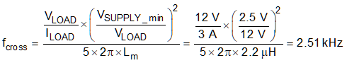
The output capacitor is required to smooth the load voltage ripple, provides an energy source during load transients and provides energy to the load during the on-time of the MOSFET. A practical way to size the output capacitor is based on the required load transient output voltage ripple specification. The load transient specification is related to the control loop crossover frequency. The control loop cross over frequency is set to 1/5th the right half plane zero frequency. This crossover frequency is calculated using Equation 15.
For this design example, the load transient specification indicates that the load voltage should not overshoot or undershoot more than 600 mV during a load transient from 50% load current (1.5 A) to 100% load current (3 A) occurs. Equation 16 is used to calculate the estimated load capacitance to achieve the specified load transient load voltage ripple requirements.

where
- ΔILOAD is the difference in the load current conditions (3 A - 1.5 A)
- ΔVLOAD is the specified overshoot voltage specification and undershoot voltage specification
The output capacitor must be rated to handle the ripple current without being damaged or without significantly reducing operating lifetime. The maximum RMS output ripple current is estimated using Equation 17. Ceramic capacitors generally have a relatively high RMS ripple current rating than electrolytic capacitors. Ceramic capacitors are used to increase the total RMS current rating of the output capacitor bank.

For this design, a total output capacitance of 200 µF is selected. The capacitor bank ESR (RESR) is estimated to be around 2 mΩ. The output capacitance and low RESR value help minimize the voltage drop during load transients.