SNVA951 November 2020 LM61460-Q1 , LM63615-Q1 , LM63625-Q1 , LM63635-Q1 , LMR33620-Q1 , LMR33630-Q1
9 Thermal Design Example
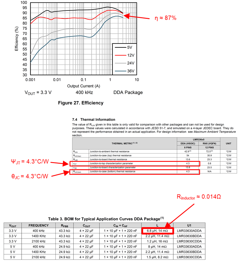
An example helps to clarify some of the ideas discussed in this paper. The LMR33630 in the HSOIC package is used. Table 9-1 summarizes the details of the design, while Figure 9-1 indicates the information needed from the data sheet.
| Device | LMR33630ADDA |
| Input Voltage | 24 V |
| Output Voltage | 3.3 V |
| Output Current | 3 A |
| Switching Frequency | 400 kHz |
| Package | HSOIC |
| Ambient Temperature | 85°C |
| TJmax | 125°C |
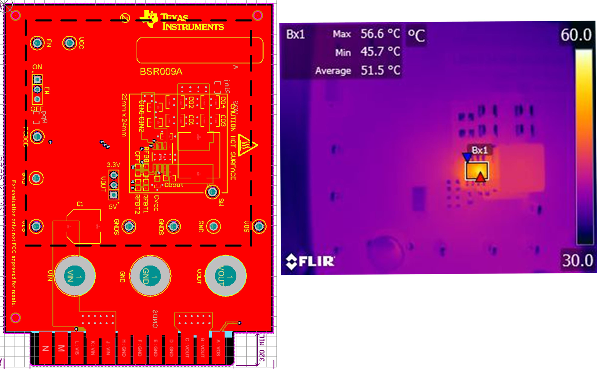
First, find the efficiency for the conditions in the application. If the efficiency for the exact conditions cannot be found, then look for data that is close and interpolate using the rules in Table 3-1. An efficiency of about 87% is found at an ambient of 25°C, and this includes the inductor loss. Reduce this to 85% to take into account the 85°C ambient in the example. The power dissipation is calculated to be about 1.7 W using Equation 2. From Equation 3 and the inductor resistance found in the data sheet, correct this power down to about 1.57 W. Next, rearrange Equation 1 to determine the maximum θJA that can be tolerated for our example conditions. This gives about 25°C/W; use 24°C/W to be conservative. Using the spreadsheet shown in Section 7.2, with the example values, adjust the size of the PCB until a value of about 24°C/W is reached. This gives a board size of about 4.84 in2, or about 30 cm2. To compare, the guideline in Equation 5 gives an area of about 25 cm2; or about 20% less. Table 9-2 summarizes the results. Figure 9-2 shows the results of thermal measurements on the LMR33630ADDA EVM, using a thermal camera and Table 9-3 tabulates the results. The comparison with the calculations will be made on the basis of θJA, since the measurements were taken at 25°C. The camera gives a top case temperature of about 56°C; using Equation 6, a TJ of about 63°C is calculated. Rearranging Equation 1, and using 25°C as the ambient when the measurement was made, θJA ≈ 24°C/W.
 Figure 9-1 Design Example Information
From Data Sheet
 Figure 9-2 PCB Measurements for Design
Example
Figure 9-2 PCB Measurements for Design
Example| Efficiency | 0.87 |
| Total Power Loss | 1.7 W |
| Inductor Loss | ≈ 0.13 W |
| Converter Loss | 1.57 W |
| Max. θJA (for TJ = 125°C and TA = 85°C) | ≈ 25°C/W → 24°C/W |
| Effective Copper Area from Spreadsheet | ≈ 30 cm2 |
| Effective Copper Area from Equation 5 | ≈ 25 cm2 |
| Case Top Temperature | 56°C |
| Estimated Junction Temperature | 63°C |
| Calculated θJA | 24°C/W |
| Total EVM PCB Area | ≈ 59 cm2 |
| Approx. Area of Inductor and IC Package | ≈ 1.44 cm2 + 0.2 cm2 = 1.64 cm2 |
| Approx. Thermal Footprint of Heat sources | ≈ 18 · 1.64 cm2 = 29 cm2 |
Notice that the total EVM area is almost 60 cm2, or nearly double that required to get a θJA of 24°C/W. This is one of those situations where some judgment and the concept of thermal foot print come in, as mentioned in Section 7. The inductor on the EVM is about 1.2 cm by 1.2 cm, while the HSOIC package is about 0.5 cm by 0.4 cm. This gives a total area of about 1.64 cm2. If this is multiplied by 18 (see Section 6) the product is about 29 cm2. This is close to the calculated value and represents the effective copper area of this PCB design. The dotted line in Figure 9-2 highlights this area. A quick glance of Figure 9-2 shows that the area within the black lines is mostly clear of any thermal bottlenecks, and seems "about right" as the effective thermal area.
The previous process can be worked from many different directions. For example you may wish to determine the maximum acceptable power loss or ambient temperature based on a given PCB area. Hopefully, the previous example will provide guidance to help the designer estimate thermal performance in any given situation.