SNVA951 November 2020 LM61460-Q1 , LM63615-Q1 , LM63625-Q1 , LM63635-Q1 , LMR33620-Q1 , LMR33630-Q1
5 PCB Copper Heat Sink
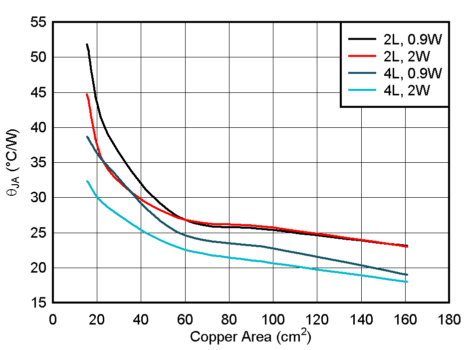
As mentioned, the PCB copper planes act as heat sinks for the regulator. The area and thickness (weight) of the copper is important. Most of the heat will be dissipated to ambient through the layer that is on the same side as the converter. The DAP must be firmly soldered directly to this plane providing both a good thermal and electrical connection. Most data sheets provide curves of overall thermal resistance (θJA) versus copper area, for a very specific set of conditions. Figure 5-1 shows an example for the LM63635-Q1 in the WSON package. The important point brought out by these curves is that more area translates into smaller thermal resistance and better thermal performance. Also, it is evident that a point-of-diminishing-return is reached at large values of copper area.
 Figure 5-1 θJA vs Copper Area for LM63635-Q1 WSON.
 There are a number of underlying assumptions for the data provided in this graph, in addition to those shown in the legend. First, using more layers helps to reduce the thermal resistance. The outside layers are the most effective in moving heat from the regulator to the outside ambient. Note that in Figure 5-1 "2L" refers to a two layer board, while "4L" refers to a four layer board. With proper thermal vias under the DAP, the heat can move through the board and to the opposite layer most effectively. The internal layers are not as effective in removing the heat, since they are somewhat shielded by the PCB material, but they do help. Next is thickness or weight of the copper. Thicker copper will give lower thermal resistance. TI recommends at least 1 oz/ft2 for top and bottom layers; and 2 oz/ft2 for power dissipation of 2 W or more. The size and number of vias is also important. The thermal resistance of each via is in parallel with its neighbor, so the overall resistance will decrease with an increasing number of vias; up to some limiting point. Thermal vias of 12-mil with 0.5 oz/ft2 copper plating is recommended. As mentioned, the most effective place for the thermal vias is under the DAP. However, placing vias around and near the regulator will also help to reduce the thermal resistance of the board. Finally, notice in Figure 5-1 that reference is made to the power dissipation in the legend. This seems strange since Equation 1 assumes that θJA remains constant with power dissipation. In fact θJA does depend somewhat on power dissipation, thus complicating the entire process of estimating, calculating, and measuring θJA. With more power dissipation you get a larger temperature drop and therefore a somewhat more efficient heat sink due to both radiation and convection. However; throughout this discussion, assume that θJA is independent of power dissipation and state what power level was assumed when estimating or measuring the thermal performance.
All of the previously-discussed considerations also apply to packages without a DAP. As stated in Section 4, it is a little more difficult to get the heat out of these types of packages. In this case the heat must flow through the relatively narrow paths through the device pins and then to the PCB. As a result, the copper leading to the VIN, SWITCH, and GND pins should be as wide as practical.