SNVA962 December 2020 TPSM5601R5H
3.3 Enable Pin (EN)
In an IBB configuration, because the EN pin is
referenced to VOUT instead of 0 V, the EN voltage thresholds are affected. In a
buck configuration, the specified typical threshold voltage for the EN pin with respect to the
return path (GND pin) of the IC is considered high at 1.2 V and low at 1.12 V. In the inverting
buck-boost configuration, however, VOUT is the reference; therefore, further
pushing the device into an enabled state. The high EN threshold is determined by 1.2 V +
VOUT and the low threshold is determined by 1.12 V + VOUT. For
example, if
VOUT = –5 V, VEN is high for
voltages above –3.8 V and low for voltages below –3.88 V.
This behavior can cause difficulties enabling or disabling the device. The level shifter alleviates any problems associated with the offset EN threshold voltages by eliminating the need for negative EN signals.
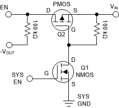
 Figure 3-3 EN Pin Level Shifter Circuit
The positive signal (SYS_EN) that originally
drove EN is instead tied to the gate of Q1 (SYS_EN). When Q1 is off (SYS_EN is grounded), Q2
detects 0 V across its VGS and also remains off. In this state, the EN pin detects
VOUT, which is below the low level threshold and
disables the device.
When SYS_EN provides enough positive voltage to turn Q1 on (gate threshold voltage as specified in the data sheet of the MOSFET), the gate of Q2 is pulled low through Q1. This drives the VGS of Q2 negative and turns Q2 on. As a consequence, VIN ties to EN through Q2, and the pin is above the high level threshold, causing the device to turn on. Make sure that the VGD of Q2 remains within the ratings of the MOSFET ratings during both enabled and disabled states. Also ensure that VGS and VDS ratings are not exceeded. Failing to adhere to these constraints can result in damaged MOSFETs.
The SYS_EN signal activates the enable circuit, and the G/D NODE signal represents the shared node between Q1 and Q2. The EN signal is the output of the circuit and goes from VIN to –VOUT properly enabling and disabling the device.