SNVA962 December 2020 TPSM5601R5H
3.2 Switching Node Behavior
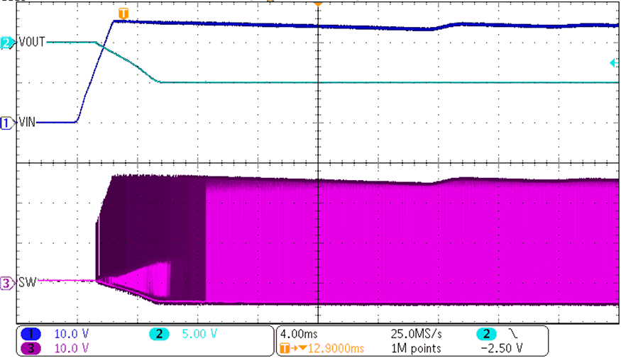
The voltage on the switch node switches from VIN to –VOUT in an inverting topology instead of VIN to GND as in a buck topology. When the high-side MOSFET turns on, the SW node detects the input voltage. When the low-side MOSFET turns on, the SW node detects the device return path, which is the negative output voltage. During start-up, VIN rises to achieve the desired input voltage, then VOUT starts ramping down after the EN pin voltage exceeds its threshold level and VIN exceeds its UVLO threshold. As VOUT continues to ramp down, the SW node low level follows VOUT down. Figure 3-2 shows the resulting normal and smooth start-up of the output voltage.
 Figure 3-2 SW Node Voltage During Start-Up