SNVAA70 june 2023 LM5176 , LM5176-Q1
3.1 TEC Current Versus Output Voltage
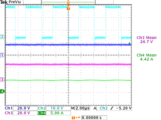
Figure 3-1, Figure 3-2, and Figure 3-3 show the waveform of Vout, SW1, SW2, and ITEC when Vout < Vin. The maximum voltage applied to the TEC element is about +10 V and ITEC is tested up to 4.34 A. Figure 3-4, Figure 3-5, and Figure 3-6 show the waveforms of LM5176 when Vout > Vin. In contrast to above, the maximum voltage is approximately -10 V and ITEC is up to -4.42 A.
CH1: SW1, CH2: SW2, CH3: VOUT, CH4: ITEC
CH1: SW1, CH2: SW2, CH3: VOUT, CH4: ITEC Figure 3-1 15-V Input, 5-V Output. CH1: SW1, CH2: SW2, CH3: VOUT, CH4: ITEC
 Figure 3-1 15-V Input, 5-V Output. CH1: SW1, CH2: SW2, CH3: VOUT, CH4: ITEC
CH1: SW1, CH2: SW2, CH3: VOUT, CH4: ITEC Figure 3-3 15-V Input, 13-V Output. CH1: SW1, CH2: SW2, CH3: VOUT, CH4: ITEC
 Figure 3-3 15-V Input, 13-V Output. CH1: SW1, CH2: SW2, CH3: VOUT, CH4: ITEC
CH1: SW1, CH2: SW2, CH3: VOUT, CH4: ITEC Figure 3-5 15-V Input, 21-V Output. CH1: SW1, CH2: SW2, CH3: VOUT, CH4: ITEC
 Figure 3-5 15-V Input, 21-V Output. CH1: SW1, CH2: SW2, CH3: VOUT, CH4: ITEC
CH1: SW1, CH2: SW2, CH3: VOUT, CH4: ITEC Figure 3-2 15-V Input, 9-V Output. CH1: SW1, CH2: SW2, CH3: VOUT, CH4: ITEC
 Figure 3-2 15-V Input, 9-V Output. CH1: SW1, CH2: SW2, CH3: VOUT, CH4: ITEC
CH1: SW1, CH2: SW2, CH3: VOUT, CH4: ITEC Figure 3-4 15-V Input, 17-V Output. CH1: SW1, CH2: SW2, CH3: VOUT, CH4: ITEC
 Figure 3-4 15-V Input, 17-V Output. CH1: SW1, CH2: SW2, CH3: VOUT, CH4: ITEC
CH1: SW1, CH2: SW2, CH3: VOUT, CH4: ITEC Figure 3-6 15-V Input, 25-V Output. CH1: SW1, CH2: SW2, CH3: VOUT, CH4: ITEC
 Figure 3-6 15-V Input, 25-V Output. CH1: SW1, CH2: SW2, CH3: VOUT, CH4: ITEC