SNVAA71 October 2023 TPSM63610
4 Typical Performance
Unless otherwise stated, the following conditions apply: VIN = 24 V , TA = 25°C.
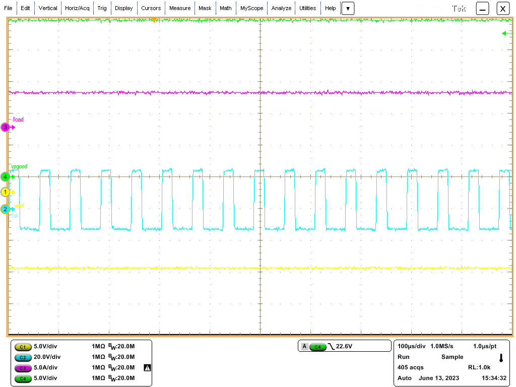
 Figure 4-1 Efficiency
 Figure 4-3 Start-up with 3-A Load at -12
Vout
 Figure 4-5 Load Transient With 2.5-A to 5-A
Load Step at -12 Vout
 Figure 4-2 Typical 5-V Output
Regulation
 Figure 4-4 Shutdown with 3-A Load at -12
Vout
 Figure 4-6 Output Voltage Ripple with 3-A Load
at -12 Vout