SNVAA73 may 2023 LM53602 , LM53602-Q1 , LM53603-Q1 , LM63625-Q1 , LM63635-Q1 , LMR14020-Q1 , LMR14030-Q1
1 Introduction
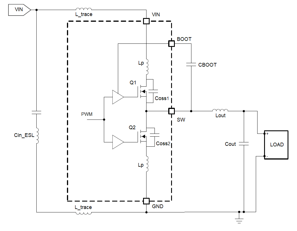
The circuit in Figure 1-1 shows the power-stage components for a synchronous buck converter. The parasitic inductance and capacitance responsible for switch-node ringing is included in this model.
 Figure 1-1 Power Stage Components
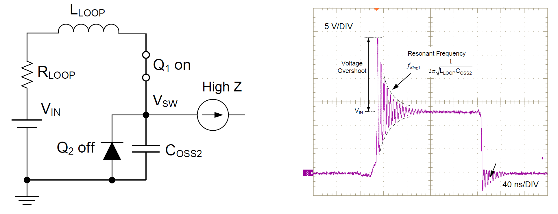
When the LS gate signal goes LOW, the low-side MOSFET turns off and the inductor current flows through the body diode of the low side MOSFET. After a short dead time, the high-side MOSFET is turned on and current flows to force the body diode of the low-side MOSFET off. As the body diode undergoes reverse recovery, the voltage on SW begins to rise and the ringing waveform results from the interaction of parasitic inductance and the switch-node capacitance. This interaction primarily consists of the Coss2 of the low-side MOSFET, as shown in Figure 1-2.
 Figure 1-2 Switch-node Ringing
This ringing not only increases MOSFET switching loss and the peak drain-to-source voltage spike, the ringing also affects broadband EMI in the 50 MHz to 300 MHz range. The ringing must be monitored and controlled within the data sheet limits of the device voltage ratings to maintain reliable operation.