SNVAA73 may 2023 LM53602 , LM53602-Q1 , LM53603-Q1 , LM63625-Q1 , LM63635-Q1 , LMR14020-Q1 , LMR14030-Q1
5.2 Refresh Boot Capacitor
In applications with short off times, resulting from high duty-cycle applications or high switching frequency, the boot capacitor can not be fully charged in each cycle if the boot resistor is too large. For these reasons, the value of the boot resistor must be kept small and must be tested and evaluated completely under all conditions of Vin, Vout, Iout, and operating temperature to achieve robust performance.
The charging current is not only limited by the RBOOT, but also limited by the parasitic inductors on the charging loop. Figure 5-2 shows the simplified block of the CBOOT charging loop of LM53602. Lparasitic is small proportion of the total parasitic inductance. Because of the 2-MHz switching frequency, the CBOOT never charges back to VCC. Simulations results show that with Lparasitic at only a few nHs and RBOOT at 10 Ω, V1 goes lower and lower over time and hits UVLO in the worst case. RBOOT at 6.8 Ω or lower is suggested for operating the LM53602 at 2 MHz frequency.
 Figure 5-2 Refresh CBOOT
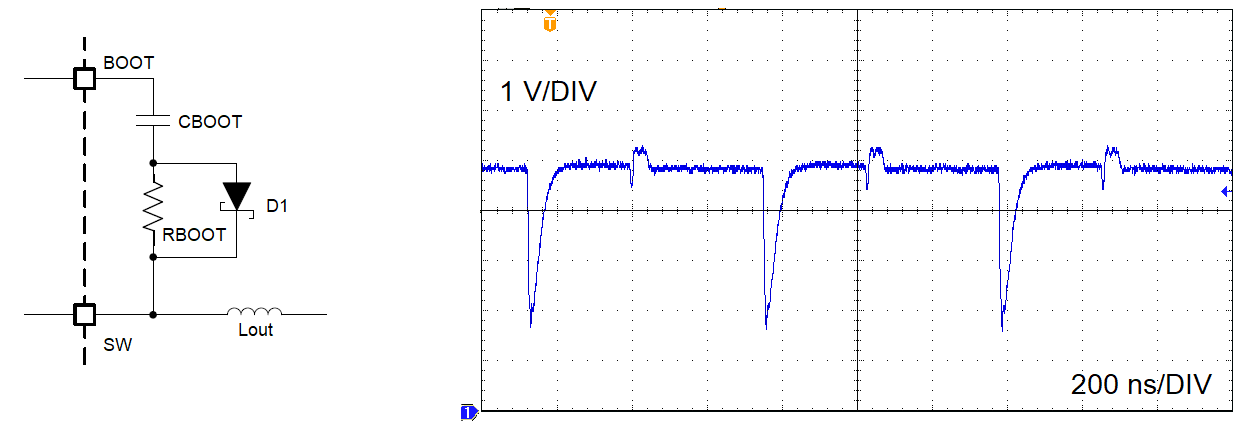
A larger RBOOT can be used if a small Schottky diode is paralleled with RBOOT which bypasses the RBOOT pin during the CBOOT charging period, as shown in Figure 5-3. The CBOOT capacitor can be charged up to 10 ns, which is shorter than the typical T-off_min of most buck converters of 100 ns to 200 ns.
 Figure 5-3 Parallel Diode With RBOOT