SNVAA76 june 2023 TPS7H4010-SEP
3 Testing Results
Testing was done at -12 V, -6 V, and -1.8 V to show the range that the inverting buck-boost topology for the TPS7H4010-SEP is capable of. Testing for the -6-V rail and -1.8 V was done with a 5-V input voltage on top of the 12-V input to show behaviors at a lower input voltage as well. Typical waveforms and testing results for each of the rails tested are shown in the following figures. Note that each of the rails except for the 5 Vin to -6 Vout were tested up to 3 A. For the 5 Vin to -6 Vout rail, waveforms were captured at 2 A because with the EVM the regulation started to become unstable past 2.5 A. This can be optimized by changing capacitance and inductance values as mentioned in the design section. The schematic for the -1.8 V rail from the TPS7H4010EVM is shown in Figure 3-1.
Traditional methods for AC response were taken, but found to be inaccurate, thus the traditional methods were not included. The transient responses show that the device in the inverting buck-boost topology is still stable under the test conditions.
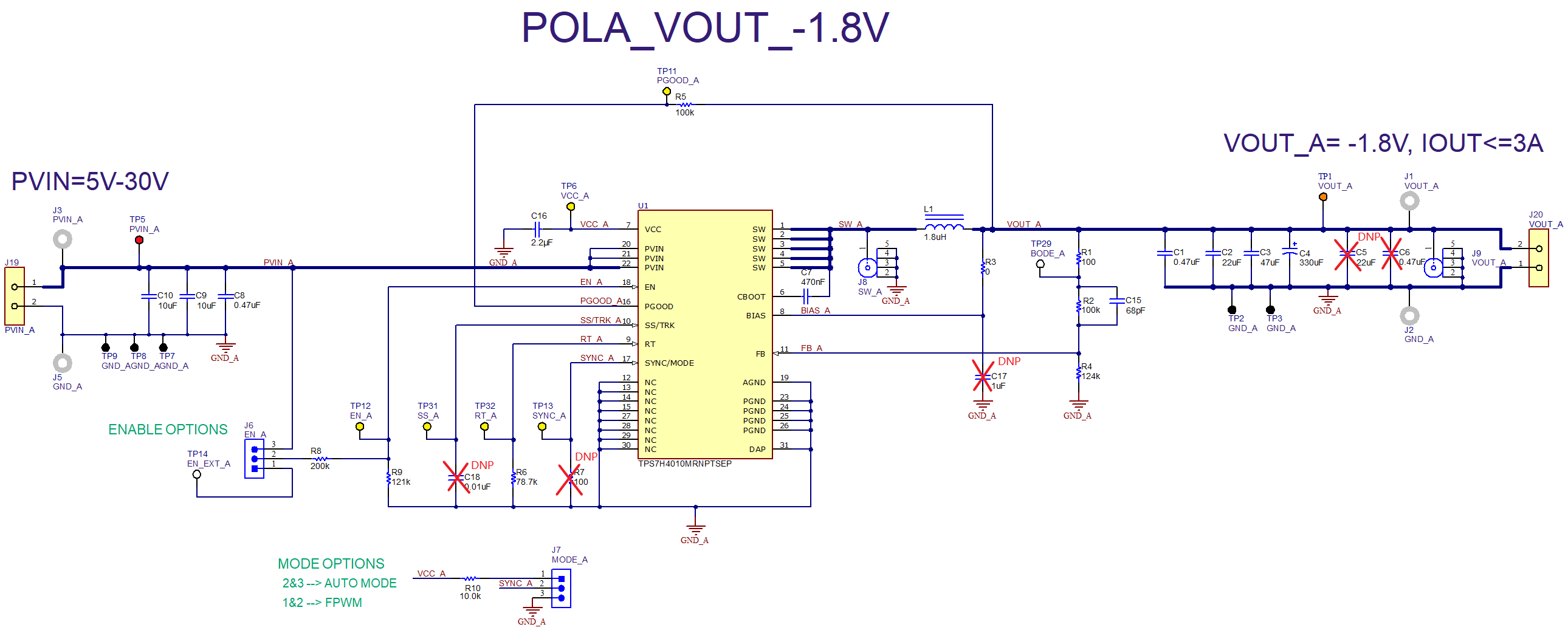 Figure 3-1 TPS7H4010EVM 1.8-V Rail Schematic
Figure 3-2 shows the tested efficiency for the 12 V in and the -12 V out from 100 mA to 3 A.
 Figure 3-2 12 V to -12 V
Efficiency
Figure 3-2 12 V to -12 V
EfficiencyFigure 3-3 shows the transient response for 12 V in and -12 V out. The output current steps from 280 mA to 2.76 A. On the positive edge of the load step, the peak of the transient is 236 mV. On the negative edge, the valley of the transient is -204 mV.
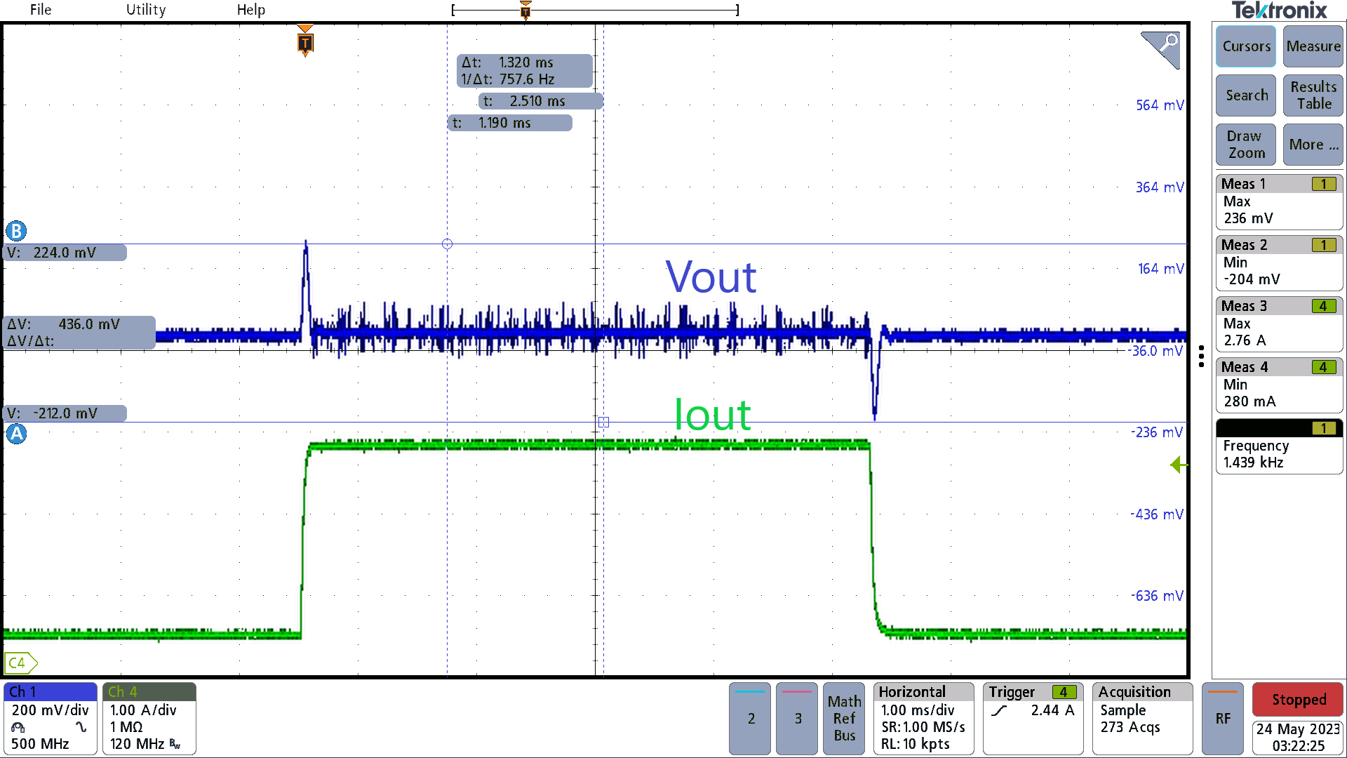 Figure 3-3 12 V to -12 V Load
Transient
Figure 3-3 12 V to -12 V Load
TransientFigure 3-4 shows the switch node for 12 V in and -12 V at a load current of 3 A. Switching frequency is 999.5 kHz
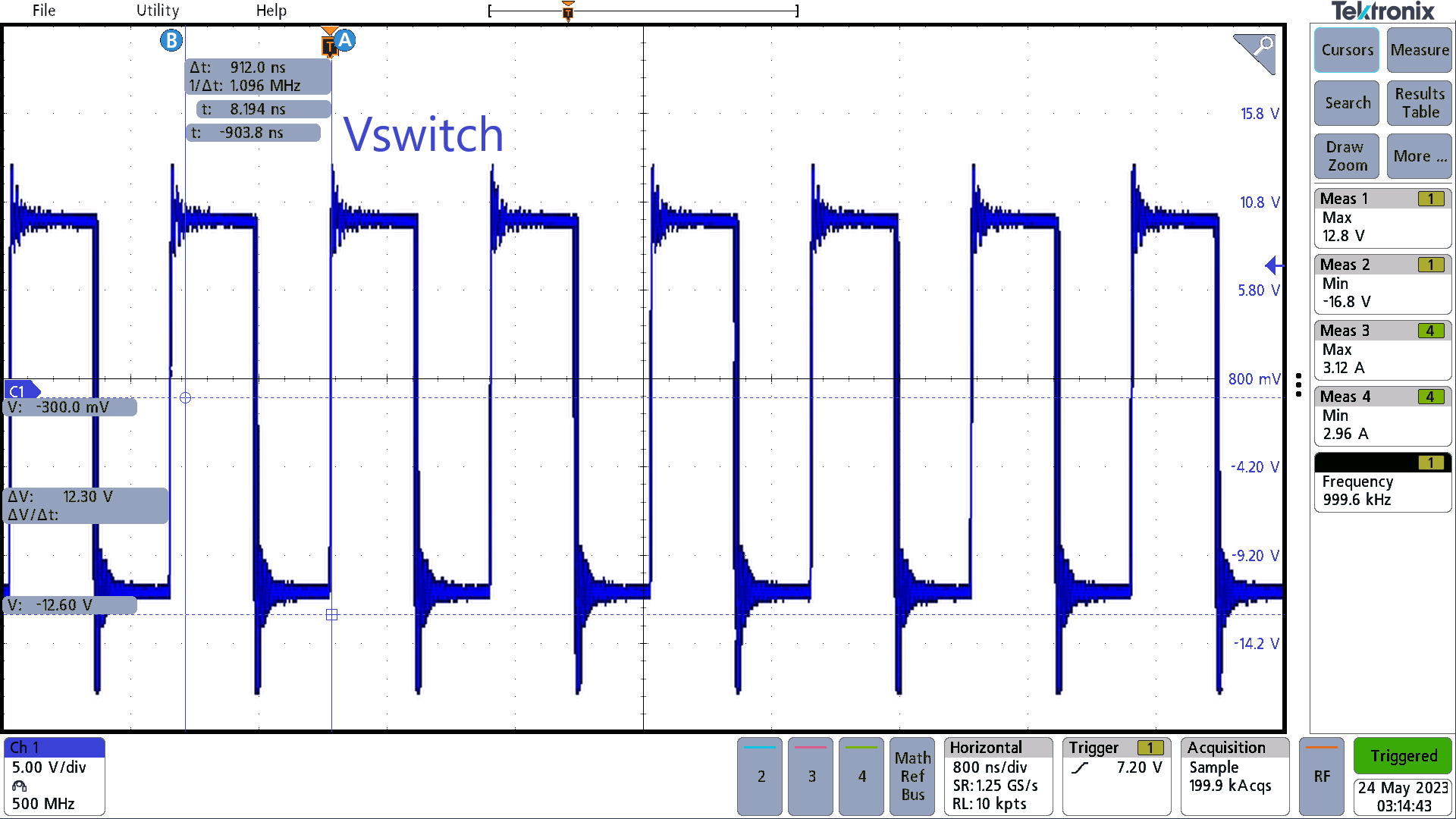 Figure 3-4 12 V to -12 V (3-A Switch
Node)
Figure 3-4 12 V to -12 V (3-A Switch
Node)Figure 3-5 shows the input ripple for 12 V in and -12 V at a load current of 3 A which is 396 mV.
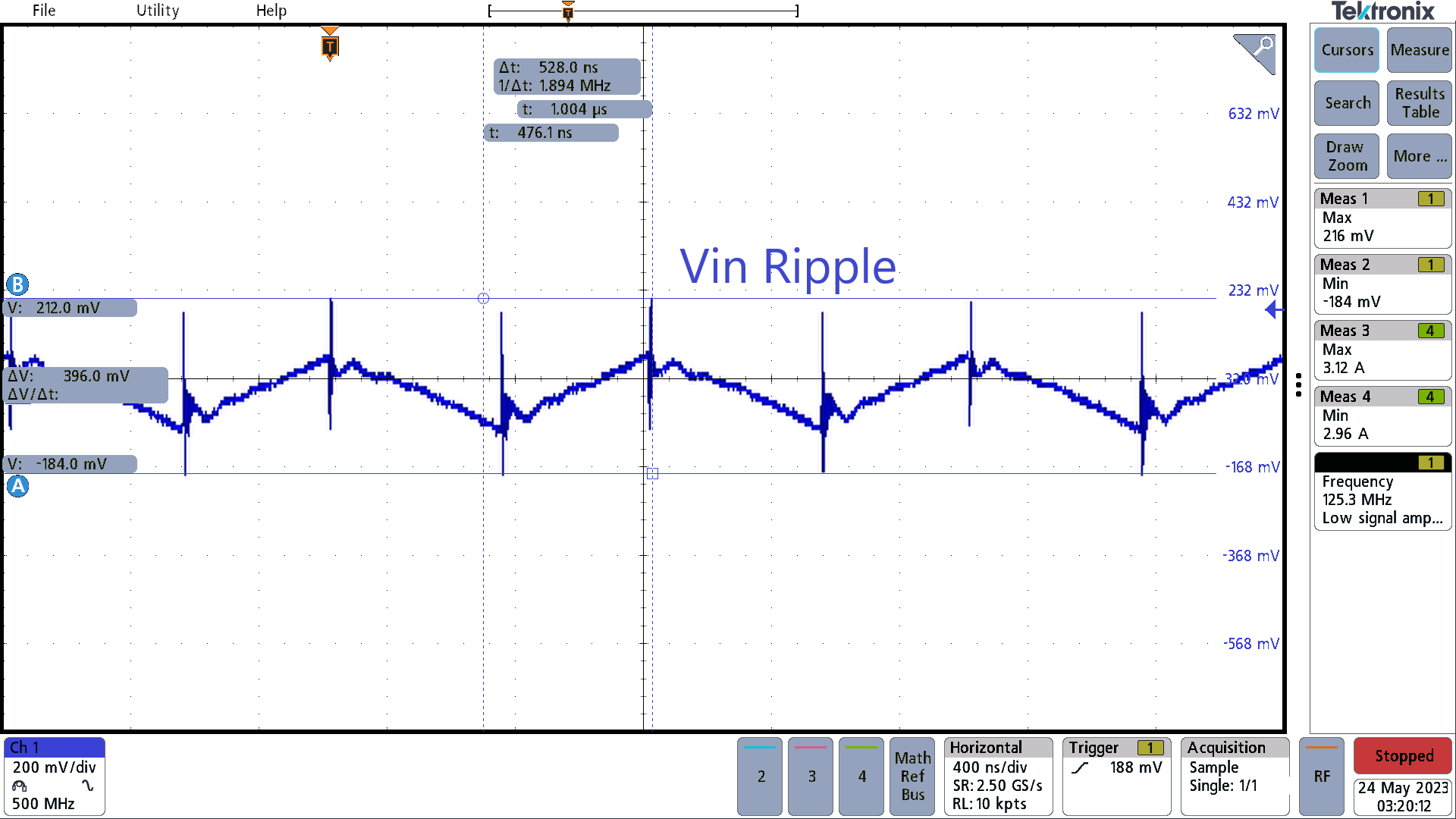 Figure 3-5 12 V to -12 V Input Ripple 3
A
Figure 3-5 12 V to -12 V Input Ripple 3
AFigure 3-6 shows the output ripple for 12 V in and -12 V at a load current of 3 A which is 115 mV.
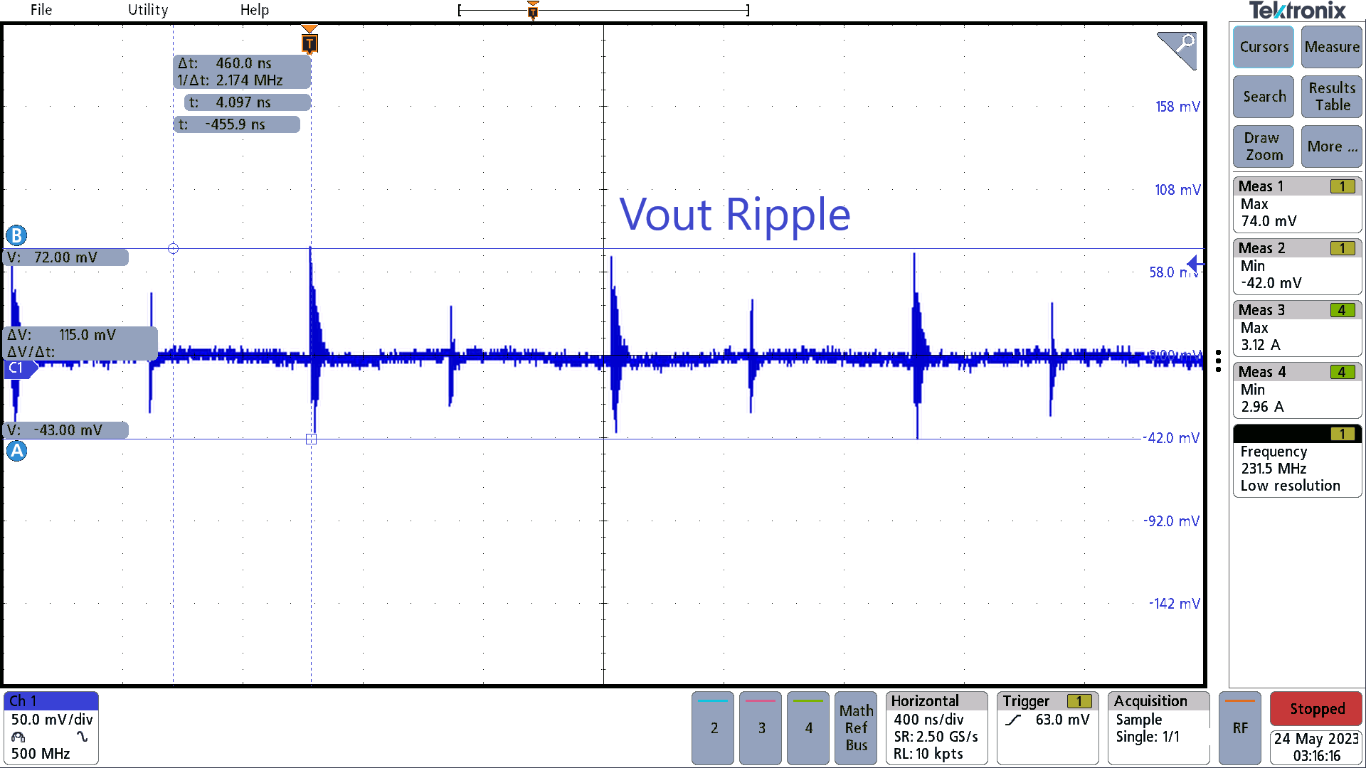 Figure 3-6 12 V to -12 V (3-A Output
Ripple)
Figure 3-6 12 V to -12 V (3-A Output
Ripple)Figure 3-7 shows the start-up waveforms of Vin and Vout. Vin takes 12.1 ms to get to 12 V and Vout takes 7.76 ms to get to -12 V.
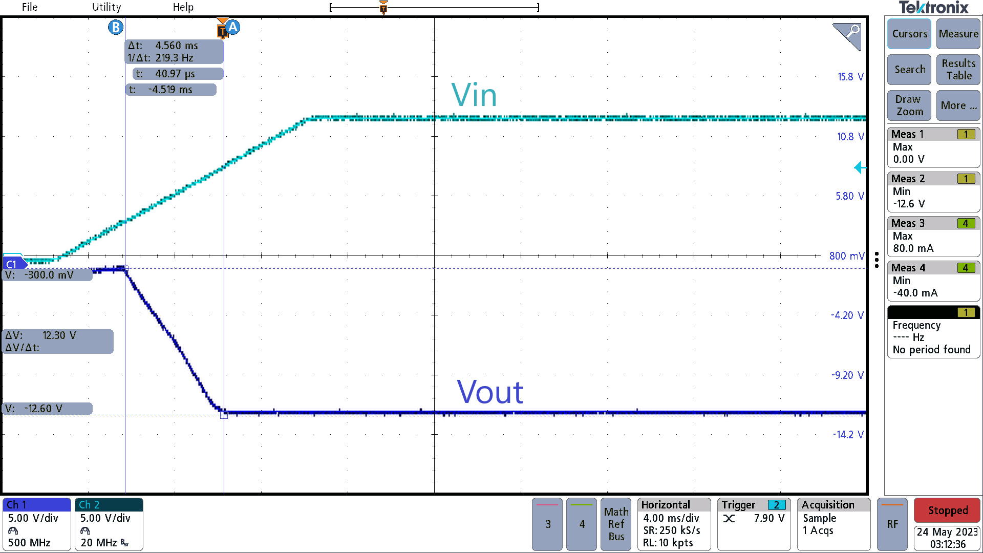 Figure 3-7 -12 V Start-up
Figure 3-8 shows the tested efficiency for the 12 V in and the -6 V out from 100 mA to 3 A.
 Figure 3-8 12 V to -6 V
Efficiency
Figure 3-8 12 V to -6 V
EfficiencyFigure 3-9 shows the transient response for 12 V in and -6 V out. The output current steps from 320 mA to 2.84 A. On the positive edge of the load step, the peak of the transient is 132 mV. On the negative edge, the valley of the transient is -60 mV.
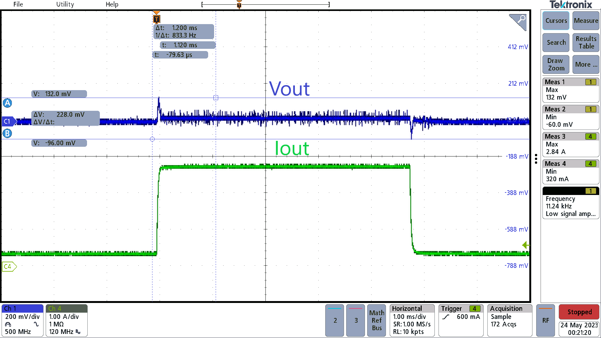 Figure 3-9 12 V to -6 V Load
Transient
Figure 3-9 12 V to -6 V Load
TransientFigure 3-10 shows the switch node for 12 V in and -6 V at a load current of 3 A. Switching frequency is 999.8 kHz.
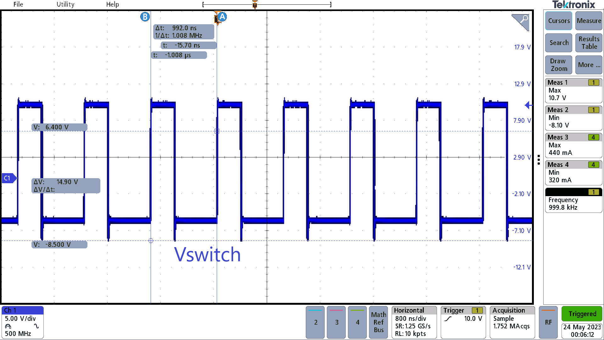 Figure 3-10 12 V to -6 V Switch Node 3
A
Figure 3-10 12 V to -6 V Switch Node 3
AFigure 3-11 shows the input ripple for 12 V in and -6 V at a load current of 3 A which is 214 mV.
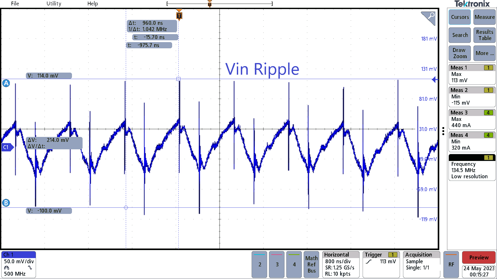 Figure 3-11 12 V to -6 V Input Ripple
3-A
Figure 3-11 12 V to -6 V Input Ripple
3-AFigure 3-12 shows the output ripple for 12 V in and -6 V at a load current of 3 A which is 94 mV.
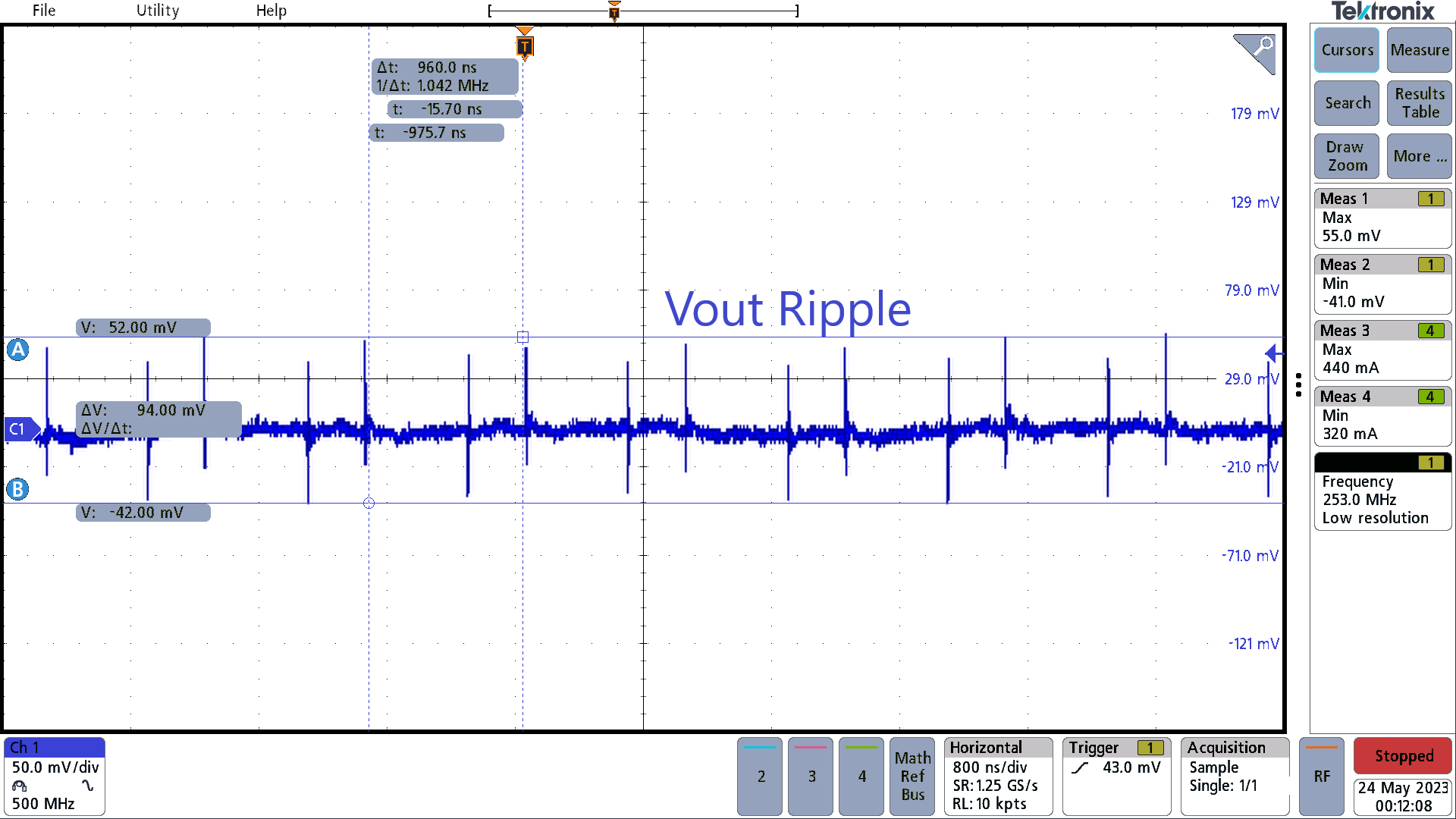 Figure 3-12 12 V to -6 V Output Ripple
3-A
Figure 3-12 12 V to -6 V Output Ripple
3-AFigure 3-13 shows the start-up waveforms of Vin and Vout. Vin takes 11.48 ms to get to 12 V and Vout takes 7.48 ms to get to -6 V.
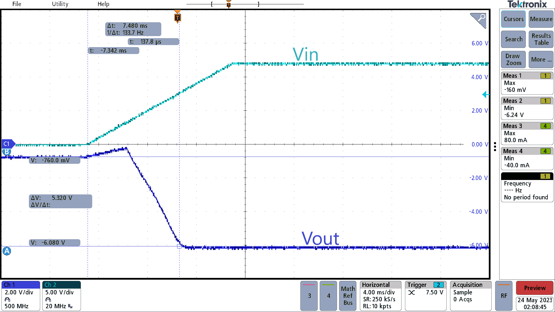 Figure 3-13 12 V to -6 V Start-up
Figure 3-14 shows the tested efficiency for the 5 V in and the -6 V out from 100 mA to 3 A.
 Figure 3-14 5 V to -6 V Efficiency
Figure 3-15 shows the transient response for 5 V in and -6 V out. The output current steps from 310 mA to 1.83 A. On the positive edge of the load step, the peak of the transient is 132 mV. On the negative edge, the valley of the transient is -68 mV.
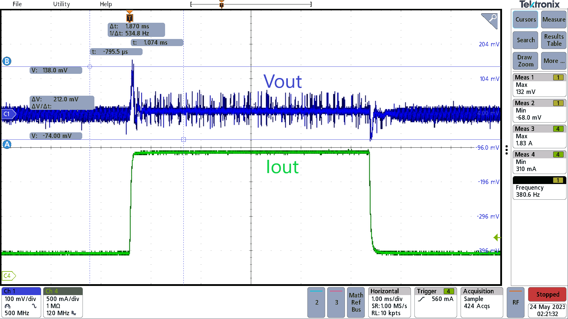 Figure 3-15 5 V to -6 V Load
Transient
Figure 3-15 5 V to -6 V Load
TransientFigure 3-16 shows the switch node for 5 V in and -6 V at a load current of 2 A. Switching frequency is 999.8 kHz.
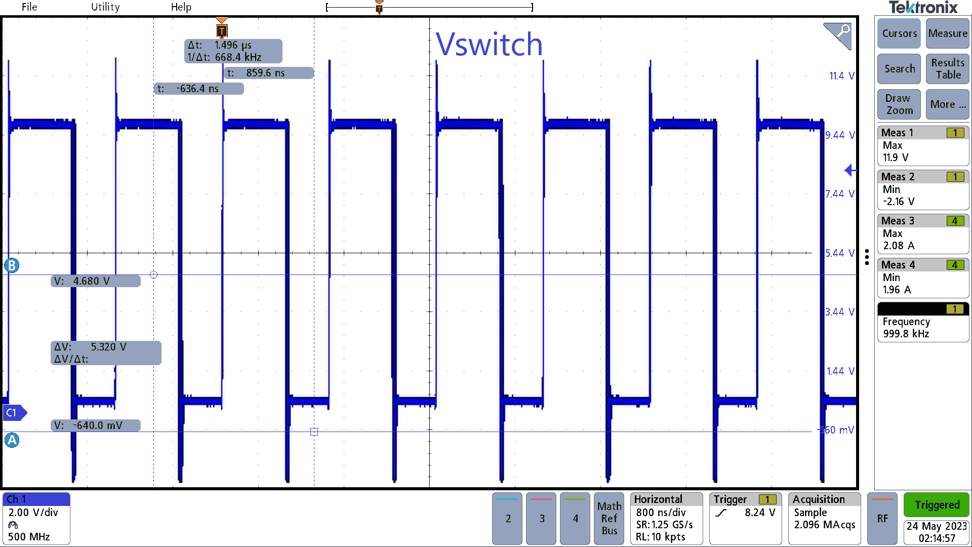 Figure 3-16 5 V to -6 V Switch Node 2
A
Figure 3-16 5 V to -6 V Switch Node 2
AFigure 3-17 shows the input ripple for 5 V in and -6 V at a load current of 2 A which is 224 mV.
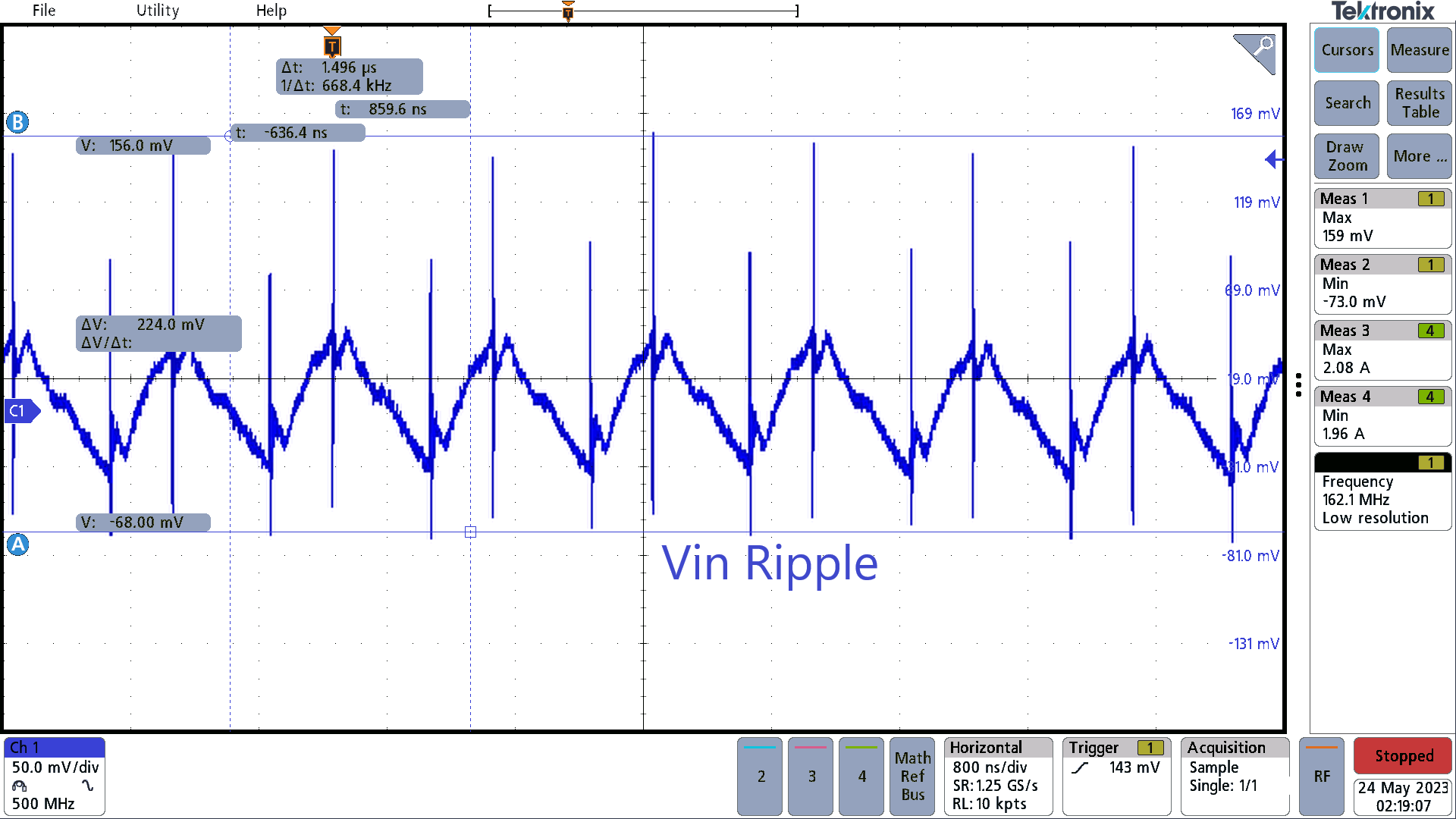 Figure 3-17 5 V to -6 V Input Ripple 2
A
Figure 3-17 5 V to -6 V Input Ripple 2
AFigure 3-18 shows the output ripple for 5 V in and -6 V at a load current of 2 A which is 97 mV.
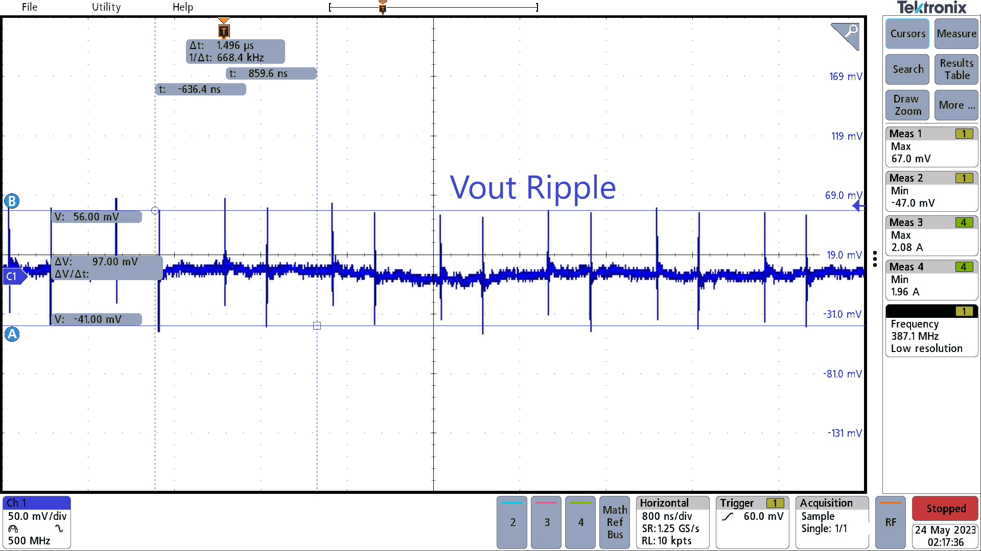 Figure 3-18 5 V to -6 V Output Ripple 2
A
Figure 3-18 5 V to -6 V Output Ripple 2
AFigure 3-19 shows the start-up waveforms of Vin and Vout. Vin takes 4.5 ms to get to 5 V and Vout takes 7.7 ms to get to -6 V.
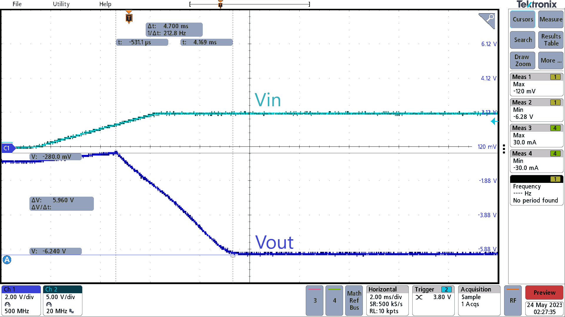 Figure 3-19 5 V to -6 V Start-up
Figure 3-20 shows the tested efficiency for the 12 V in and the -1.8 V out from 100 mA to 3 A.
 Figure 3-20 12 V to -1.8 V
Efficiency
Figure 3-20 12 V to -1.8 V
EfficiencyFigure 3-21 shows the transient response for 12 V in and -1.8 V out. The output current steps from 320 mA to 2.76 A. On the positive edge of the load step, the peak of the transient is 42 mV. On the negative edge, the valley of the transient is -12 mV
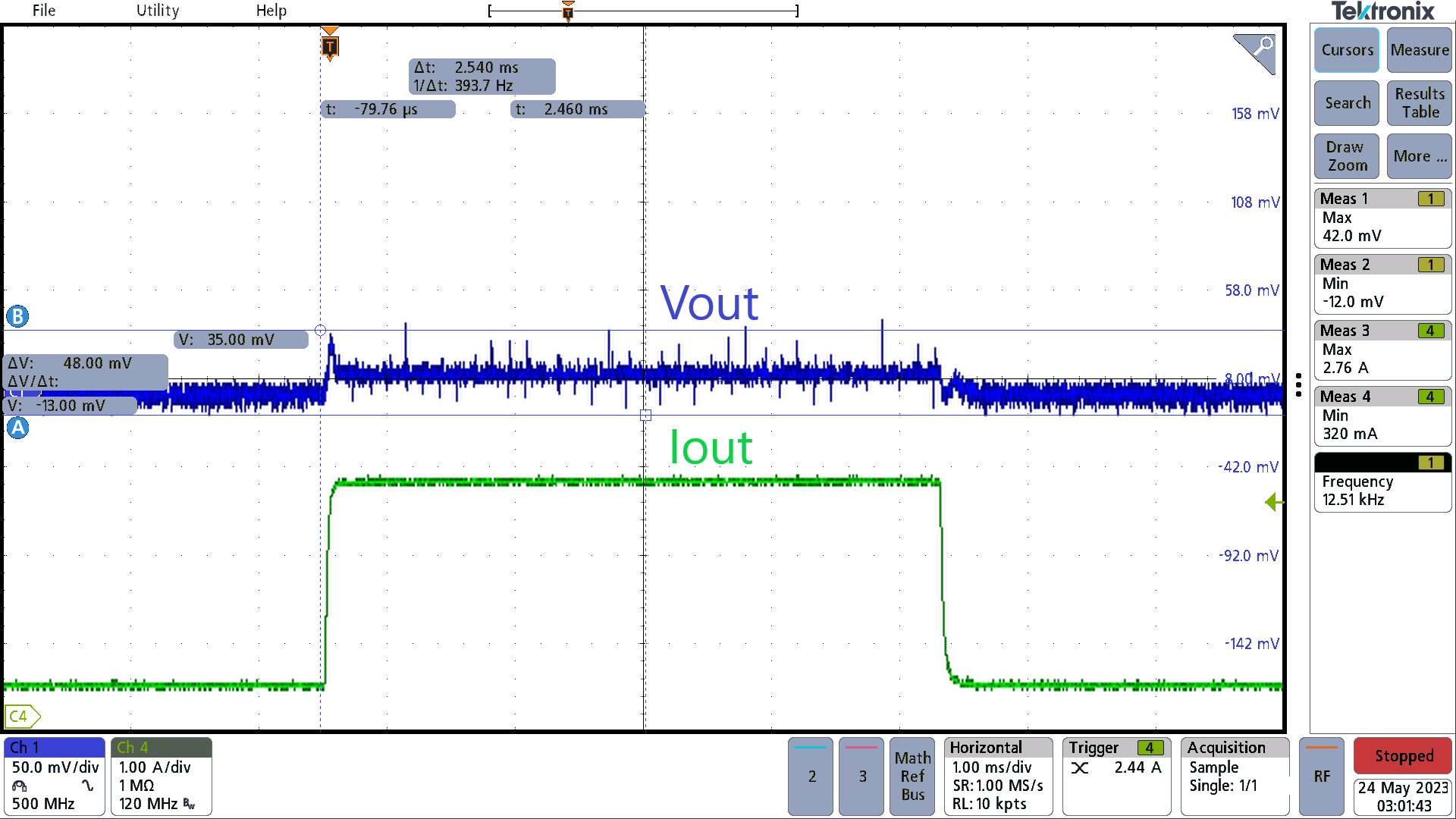 Figure 3-21 12 V to -1.8 V Load
Transient
Figure 3-21 12 V to -1.8 V Load
TransientFigure 3-22 shows the switch node for 12 V in and -1.8 V at a load current of 3 A. Switching frequency is 1.008 MHz.
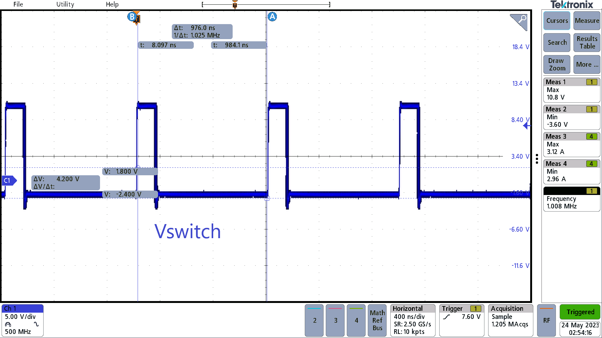 Figure 3-22 12 V to -1.8 V (Switch Node
3-A)
Figure 3-22 12 V to -1.8 V (Switch Node
3-A)Figure 3-23 shows the input ripple for 12 V in and -1.8 V at a load current of 3 A which is 190 mV.
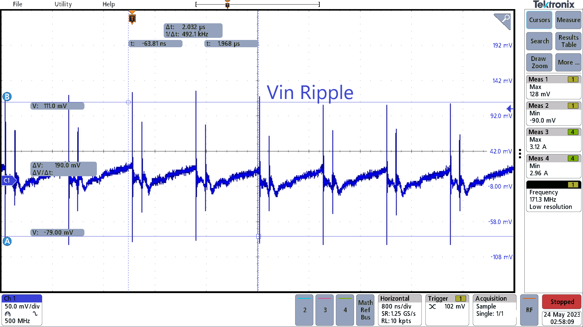 Figure 3-23 12 V to -1.8 V Input Ripple
3-A
Figure 3-23 12 V to -1.8 V Input Ripple
3-AFigure 3-24 shows the output ripple for 12 V in and -1.8 V at a load current of 3 A which is 48 mV.
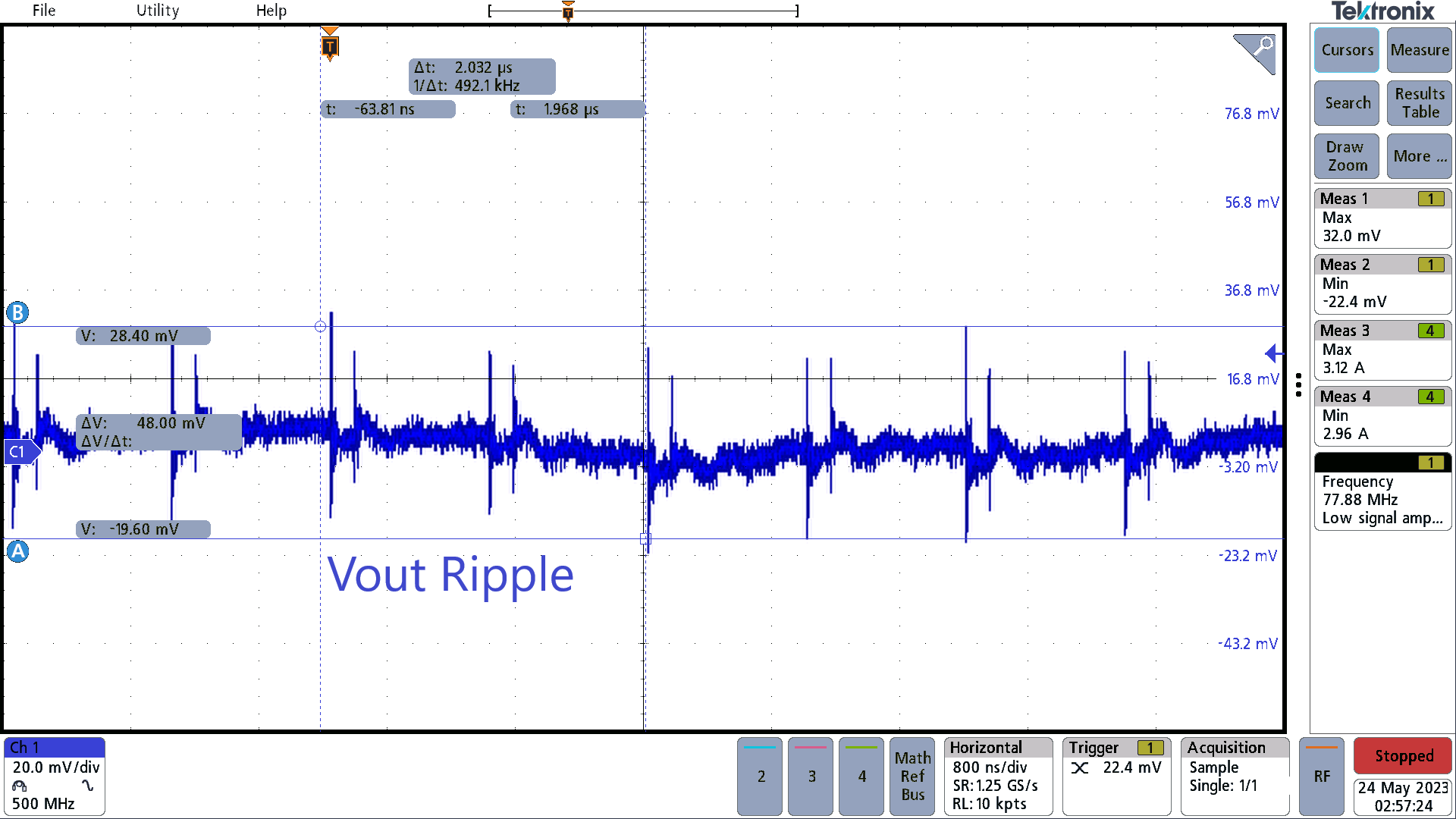 Figure 3-24 12 V to -1.8 V Output Ripple
3-A
Figure 3-24 12 V to -1.8 V Output Ripple
3-AFigure 3-25 shows the start-up waveforms of Vin and Vout. Vin takes 12.2 ms to get to 12 V and Vout takes 7.22 ms to get to -1.8 V.
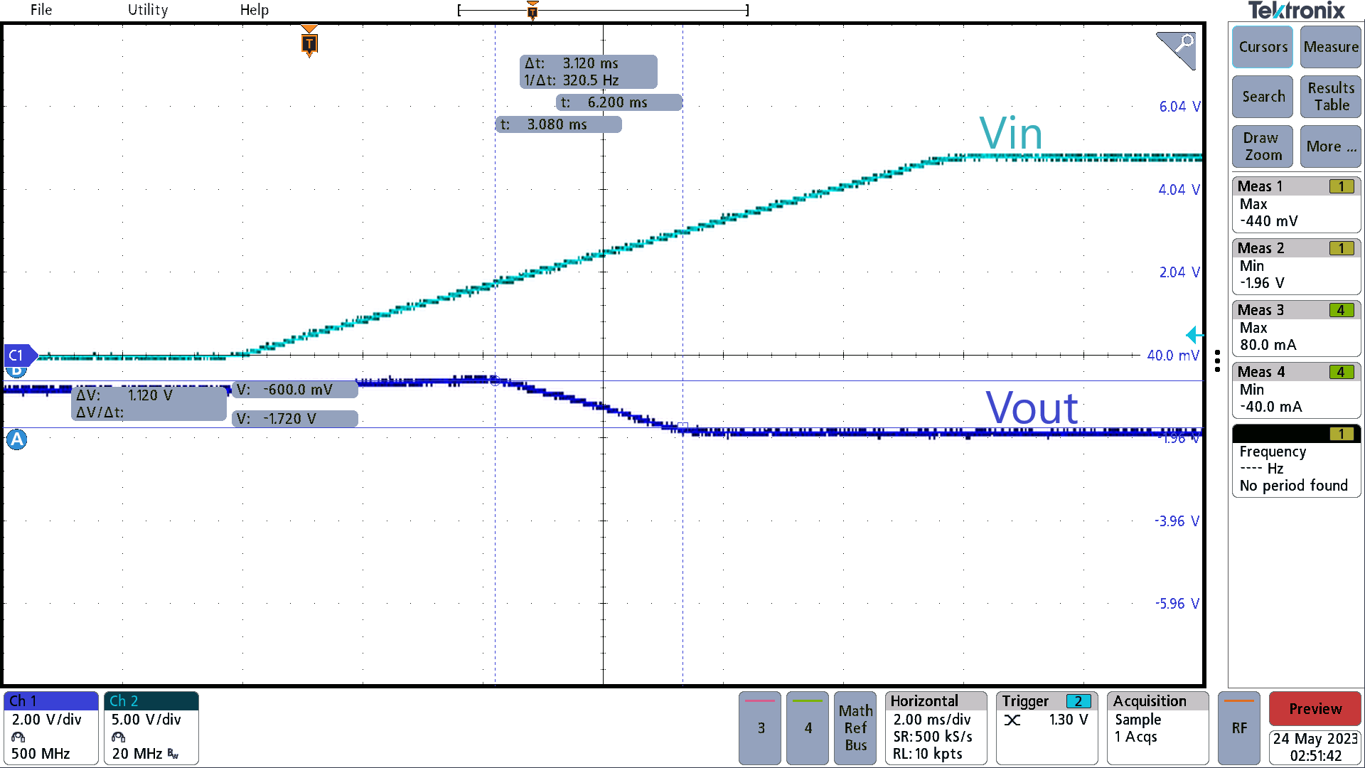 Figure 3-25 12 V to -1.8 V
Start-up
 Figure 3-26 5 V to -1.8 V
Efficiency
Figure 3-26 5 V to -1.8 V
EfficiencyFigure 3-27 shows the transient response for 5 V in and -1.8 V out. The output current steps from 320 mA to 2.76 A. On the positive edge of the load step the peak of the transient is 48 mV. On the negative edge the valley of the transient is -16 mV.
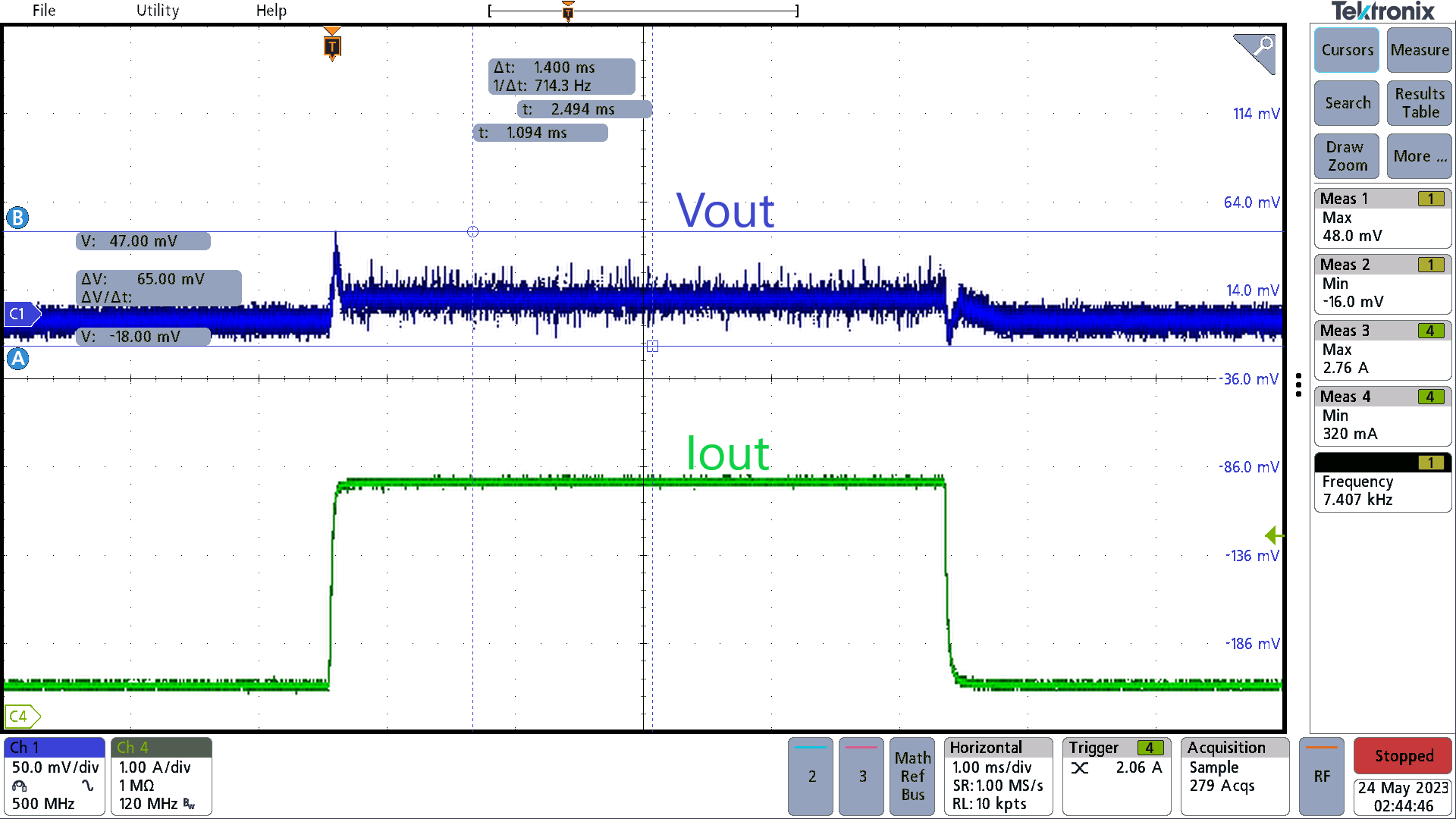 Figure 3-27 5 V to -1.8 V
Transient
Figure 3-27 5 V to -1.8 V
TransientFigure 3-28 shows the switch node for 5 V in and -1.8 V at a load current of 3 A. Switching frequency is 1.008 MHz.
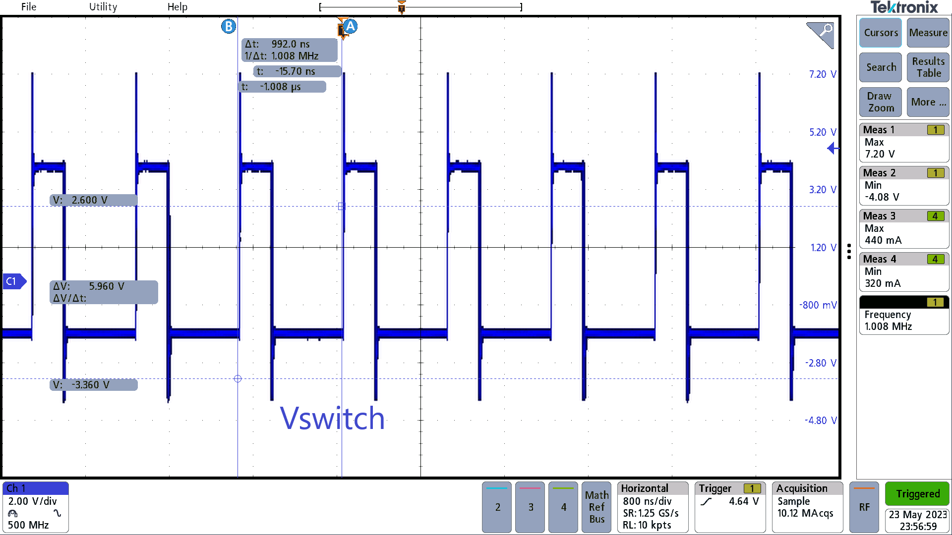 Figure 3-28 5 V to -6 V Switch Node
3-A
Figure 3-28 5 V to -6 V Switch Node
3-AFigure 3-29 shows the input ripple for 5 V in and -1.8 V at a load current of 3 A which is 264 mV.
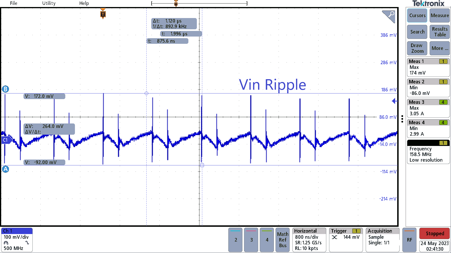 Figure 3-29 5 V to -1.8 V Input Ripple
3-A
Figure 3-29 5 V to -1.8 V Input Ripple
3-AFigure 3-30 shows the output ripple for 12 V in and -1.8 V at a load current of 3 A which is 80.8 mV.
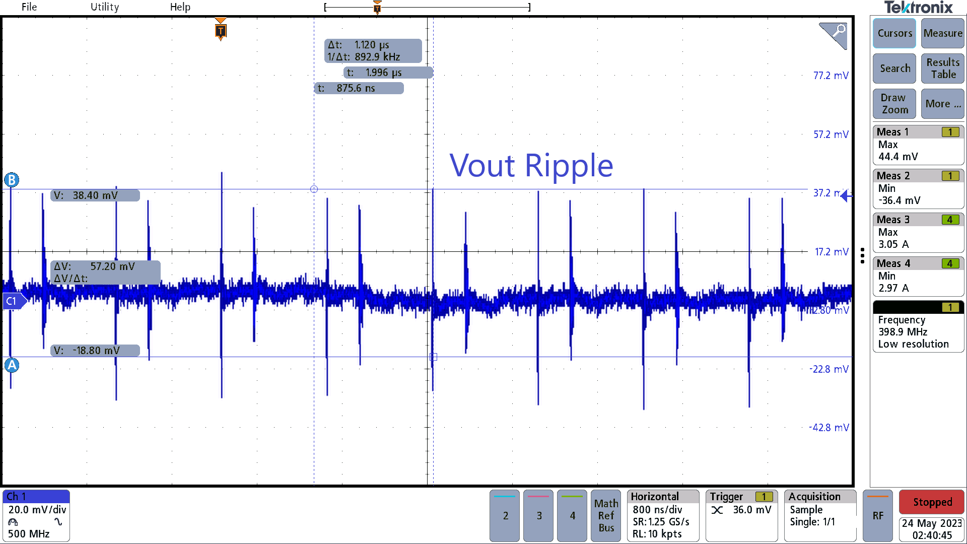 Figure 3-30 5 V to -1.8 V Output Ripple
3-A
Figure 3-30 5 V to -1.8 V Output Ripple
3-AFigure 3-31 shows the start-up waveforms of Vin and Vout. Vin takes 4.4 ms to get to 12 V, and Vout takes 7.6 ms to get to -1.8 V.
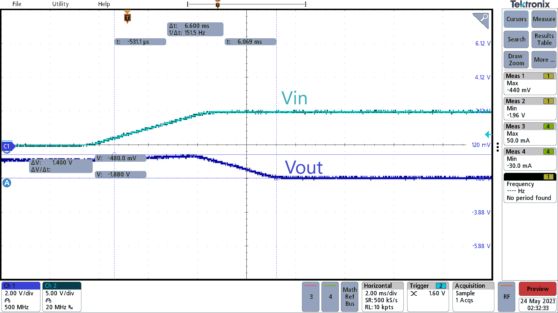 Figure 3-31 5 V to -1.8 V Start-up (Dark
Blue Vout, Light Blue Vin)