SNVAA84 October   2023 LMR36506


  1.   1
  2.   Abstract
  3.   Trademarks
  4. 1Introduction
    1. 1.1 Topology Selection
    2. 1.2 From Buck to Fly-Buck-Boost Converter
  5. 2Specific Implementation of the Fly-Buck-Boost Converter
    1. 2.1 Schematic
    2. 2.2 Bill of Materials
  6. 3Test Results
    1. 3.1 Start-up Behavior
    2. 3.2 System Loop Stability
    3. 3.3 Thermal Behavior
    4. 3.4 VOUT Ripple and SW Node Waveforms
    5. 3.5 Efficiency Data
      1. 3.5.1 Efficiency Data for Balanced Loads
      2. 3.5.2 Efficiency Data for Unbalanced Loads
    6. 3.6 Load Regulation
      1. 3.6.1 Load Regulation for Balanced Loads
      2. 3.6.2 Load Regulation for Unbalanced Loads
  7. 4Summary
  8. 5References

Start-up Behavior

Figure 3-12 shows the typical start-up behavior of fly-buck-boost configuration where the signals on the positive and negative rails ramp-up symmetrically on the supply of VIN. The pink line indicates the input voltage of 16 V and the dark and light-blue lines are the positive and negative rail signals ramping up to ±15 V symmetrically.
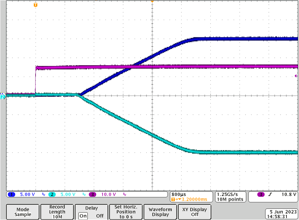
GUID-20230906-SS0I-N3LW-XMTV-2S0BCJ3WHMN2-low.png Figure 3-1 Start-up Behavior of Fly-Buck-Boost Topology