SNVAAA6 September 2024 LM61495
4.2 Inductor Selection and Maximum Output Current
The average inductor current is affected in this topology. In the buck configuration, the average inductor current is equal to the average output current because the inductor always supplies current to the load during both the ON- and OFF-times of the control MOSFET. However, in the inverting buck-boost configuration, only the output capacitor supplies the load with current, while the load is completely disconnected from the inductor during the ON-time of the control MOSFET. During the OFF-time, the inductor connects to both the output capacitor and the load (see Figure 2-2 to Figure 2-4). Because the OFF-time is 1 – D of the switching period, the average inductor current in Equation 2 is calculated as:
The duty cycle for the typical buck converter is simply VOUT / (VIN × η), but the calculation of the duty cycle in Equation 3 for an inverting buck-boost converter becomes:
Equation 4 provides the peak-to-peak inductor ripple current:
where,
- ΔIL (A): Peak-to-peak inductor ripple current
- D: Duty cycle
- fS (Hz): Switching frequency
- L (H): Inductor value
- VIN (V): Input voltage with respect to ground, not with respect to the device ground or VOUT
In the inverting buck-boost topology, the maximum output current is reduced as compared to the buck topology. This reduction is a result of the peak inductor current being higher.
The inductor for the IBB is selected based on the desired ripple current, much like any other DC/DC converter. Typically a value of between 20% and 40% of the load current is used for ΔIL. Equation 5 can be derived by Equation 4 to determine the value of L along with the maximum inductor current. This information is used to select a standard inductor that is designed for the application.
4.7μH inductor is selected in PMP23333 design. For an output voltage of – 8V and input voltage of + 12V ± 10%, the following calculations produce the maximum allowable output current that can make sure is based on the LM61495 minimum valley current limit value of 9.8A which is described in the data sheet. Due to increased duty cycles when operating at high load current, the duty cycle used for the following maximum output current calculation in Equation 6 be increased by 5% for these conditions, which provides a more accurate maximum output current calculation.
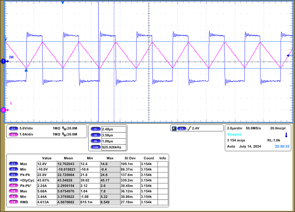
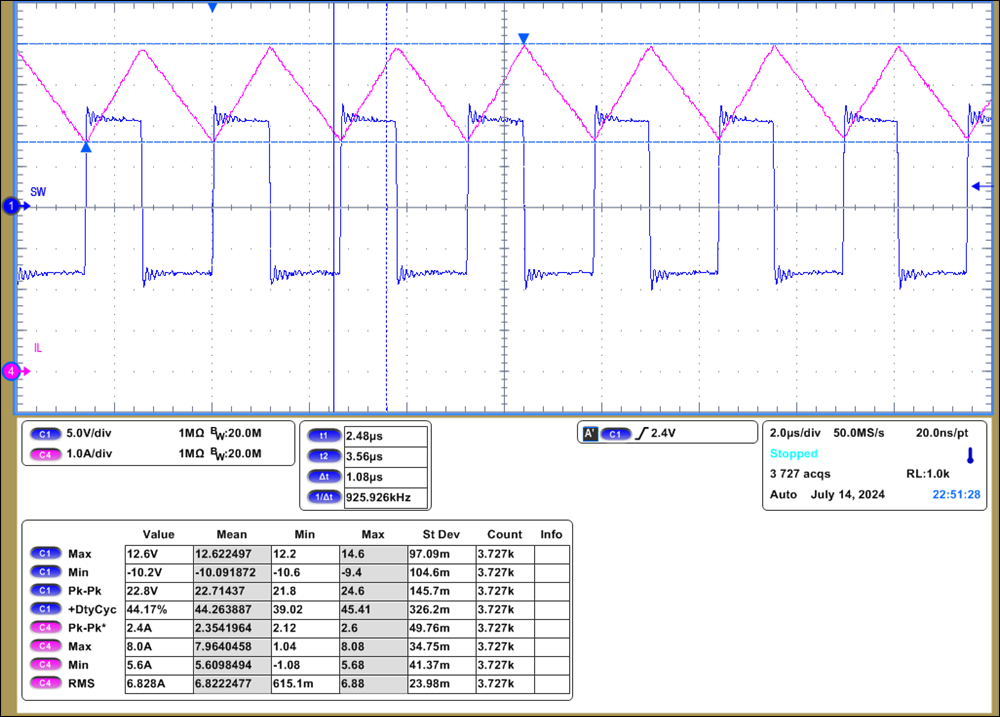
Figure 4-2 and Figure 4-3 shows the switching voltage and inductor current waveforms under - 2.7A, - 4A load conditions and shows that the calculation almost matches with real values.
 Figure 4-2 SW and IL Waveforms Under IOUT = - 2.7A
 Figure 4-3 SW and IL Waveforms Under IOUT = - 4A
To calculate allowable maximum current, IL(Valley) needs to be less than 9.8A as shown in Equation 11. Therefore, IOUT_MAX needs to be less than 5.9A as calculated in Equation 12. Even though, IOUT_MAX can be increased to 5.9A, Texas Instruments does not recommend to use higher load than 4A in this design since the higher load can cause IC thermal rising significantly.