SNVS837B June 2013 – April 2016 LM3263
PRODUCTION DATA.
- 1 Features
- 2 Applications
- 3 Description
- 4 Revision History
- 5 Pin Configuration and Functions
- 6 Specifications
-
7 Detailed Description
- 7.1 Overview
- 7.2 Functional Block Diagram
- 7.3
Feature Description
- 7.3.1 PWM Operation
- 7.3.2 PFM Operation
- 7.3.3 Active Current Assist and Analog Bypass (ACB)
- 7.3.4 Bypass Operation
- 7.3.5 Dynamic Adjustment of Output Voltage
- 7.3.6 DC-DC Operating Mode Selection
- 7.3.7 Internal Synchronous Rectification
- 7.3.8 Current Limit
- 7.3.9 Timed Current Limit
- 7.3.10 Thermal Overload Protection
- 7.3.11 Start-Up
- 7.4 Device Functional Modes
- 7.5 Programming
- 7.6 Register Map
- 8 Application Information
- 9 Power Supply Recommendations
- 10Layout Considerations
- 11Device and Documentation Support
- 12Mechanical, Packaging, and Orderable Information
7 Detailed Description
7.1 Overview
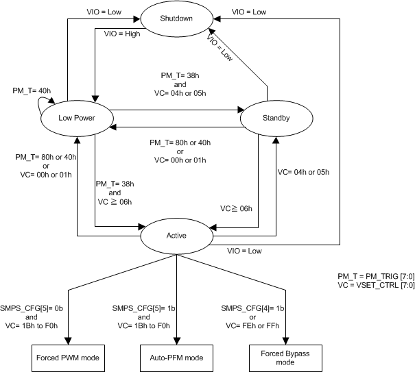
The LM3263 is a high-efficiency step-down DC-DC converter optimized to power the RF power amplifier (PA) in cell phones, portable communication devices, or battery-powered RF devices with a single litium-Ion battery. It operates in modulated-frequency pulsed width modulation (PWM) mode for 2G transmissions (with MODE = Forced PWM (PWM only), register 01h SMPS_CFG [5] set to 0b), automatic mode transition between pulse frequency modulation (PFM) and PWM for 3G/4G RF PA operation (with MODE = Auto-PFM (PFM/PWM), SMPS_CFG bit 5 set to 1b), or forced-bypass mode (with SMPS_CFG [4] set to 1b or REGISTER_0 [6:0] set to 7Fh or register 03h VSET_CTRL [7:0] set to FEh-FFh). Power states are also in provided shutdown, low power, standby, and active modes. The DC-DC converter operates at active mode. Please see Figure 21 and Register Map.
PWM mode provides high efficiency and very low output-voltage ripple. In PWM-mode operation, the modulated switching frequency helps to reduce RF transmit noise. In PFM mode, the converter operates with reduced switching frequencies and lower supply current to maintain high efficiencies. The forced-bypass mode allows the user to drive the output directly from the input supply through a bypass FET. The shutdown mode turns the LM3263 off and reduces current consumption to 0.02 µA (typical).
In the PWM and PFM modes of operation, the output voltage of the LM3263 can be dynamically programmed from 0.4 V to 3.6 V (typical) by setting the VSET register. Current overload protection and thermal overload protection are also provided.
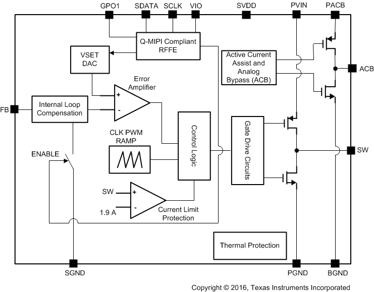
The LM3263 was engineered with Active Current assist and analog Bypass (ACB). This unique feature allows the converter to support maximum load currents of 2.5 A (minimum) while keeping a small footprint inductor and meeting all of the transient behaviors required for operation of a multi-mode RF PA. The ACB circuit provides an additional current path when the load current exceeds 1.45 A (typical) or as the switcher approaches dropout. Similarly, the ACB circuit allows the converter to respond with faster VSET output voltage transition times by providing extra output current on rising and falling output edges. The ACB circuit also performs the function of analog bypass. Depending upon the input voltage, output voltage, and load current, the ACB circuit automatically and seamlessly transitions the converter into analog bypass, while maintaining output voltage regulation and low output voltage ripple. Full bypass (100% duty cycle operation) occurs if the total dropout resistance in bypass mode (Rtot_drop = 45 mΩ) is insufficient to regulate the output voltage.
The device 16-pin DSBGA package is the best solution for space-constrained applications such as cell phones and other hand-held devices. The high switching frequency, 2.7 MHz (typical) in PWM mode, reduces the size of input capacitors, output capacitor, and of the inductor. Use of a DSBGA package is best suited for opaque case applications and requires special design considerations for implementation (see Layout Considerations).
7.2 Functional Block Diagram
7.3 Feature Description
7.3.1 PWM Operation
The LM3263 operates in PWM mode when forced-PWM mode operation is selected (SMPS_CFG [5] set to 0b). The switching frequency is modulated, and the switcher regulates the output voltage by changing the energy per cycle to support the load required. During the first portion of each switching cycle, the control block in the LM3263 turns on the internal PFET switch. This allows current to flow from the input through the inductor and to the output filter capacitor and load. The inductor limits the current to a ramp with a slope of (VBATT – VSET)/L, by storing energy in its magnetic field.
During the second portion of each cycle, the control block turns the PFET switch off, blocking current flow from the input, and then turns the NFET synchronous rectifier on. The inductor draws current from ground through the NFET and to the output filter capacitor and load, which ramps the inductor current down with a slope of –VSET/L. The output filter capacitor stores charge when the inductor current is greater than the load current and releases it when the inductor current is less than the load current, smoothing the voltage across the load.
At the next rising edge of the clock, the cycle repeats. An increase of load pulls the output voltage down, increasing the error signal. As the error signal increases, the peak inductor current becomes higher therefore increasing the average inductor current. The output voltage is therefore regulated by modulating the PFET switch on time to control the average current sent to the load. The circuit generates a duty-cycle modulated rectangular signal that is averaged using a low pass filter formed by the inductor and output capacitor. The output voltage is equal to the average of the duty-cycle modulated rectangular signal.
7.3.2 PFM Operation
When auto-PFM mode operation is selected (SMPS_CFG [5] set to 1b), the LM3263 automatically transitions from PWM operation into PFM operation if the average inductor current is less than 60 mA (minimum) and the difference between VBATT – VSET ≥ 0.6 V. The switcher regulates the fixed output voltage by transferring a fixed amount of energy during each cycle and modulating the frequency to control the total power delivered to the output. The converter switches only as needed to support the demand of the load current, therefore maximizing efficiency. If there is an increase in load current during PFM mode to more than 120 mA (typical), the part automatically transitions into PWM mode. A 20 mA (typical) hysteresis window exists between PFM and PWM transitions. After a transient event, the part temporarily operates in PWM mode to quickly charge or discharge the output. This is true for start-up conditions or if the mode operation is changed from forced-PWM to auto-PFM mode (SMPS_CFG [5] toggled from 0b to 1b). Once the output reaches its target output voltage, and the load is less than 60 mA (minimum), then the device seamlessly transitions into PFM mode (assuming the device is not in forced-bypass condition).
7.3.3 Active Current Assist and Analog Bypass (ACB)
The 3GPP time mask requirement for 2G requires high current to be sourced by the LM3263. These high currents are required for a small time during transients or under a heavy load. Overrating the switching inductor for these higher currents increases the solution size and is not an optimum solution. Thus, to allow an optimal inductor size for such a load, an alternate current path is provided from the input supply through the ACB pin. Once the switcher current limit ILIM,PFET,SteadyState is reached, the ACB circuit starts providing the additional current required to support the load. The ACB circuit also minimizes the dropout voltage by having the analog bypass FET in parallel with VSET. The LM3263 can provide up to 2.5 A (minimum) of current in bypass mode.
7.3.4 Bypass Operation
The bypass circuit provides an analog bypass function with very low dropout resistance (Rtot_drop = 45 mΩ typical). When SMPS_CFG [4] is set to 0b, the part is in automatic bypass mode which automatically determines the amount of bypass needed to maintain voltage regulation. When the input supply voltage to the LM3263 is lowered to a level where the commanded duty cycle is higher than what the converter is capable of providing, the part goes into pulse-skipping mode. The switching frequency is reduced to maintain a low and well behaved output voltage ripple. The analog bypass circuit allows the converter to stay in regulation until full bypass is reached (100% duty cycle operation). The converter comes out of full bypass and back into analog bypass regulation mode with a similar reverse process.
To operate the device at the Forced-Bypass mode, set REGISTER_0 to 7Fh or VSET_CTRL to FEh-FFh.
7.3.5 Dynamic Adjustment of Output Voltage
The LM3263 can be dynamically programmed to an output voltage from 0.4 V to 3.6 V with 30 mV or 15 mV steps. REGISTER_0 [6:0] is set to 0Dh to 78h with 30-mV output voltage steps, and VSET_CTRL [7:0] is set to 1Bh to F0h with 15-mV steps. Although the output voltage can be programmed lower than 0.4 V and higher than 3.6 V by setting the registers, the device might suffer from larger output ripple voltage, higher current limit operation, and decreased linearity.
7.3.6 DC-DC Operating Mode Selection
Programming SMPS_CFG [5] changes the state of the converter to one of the two allowed modes of operation. SMPS_CFG [5] default is 0b, and the device operates in forced-PWM mode (PWM only). Setting the register bit to 1b sets the device for automatic transition between PFM/PWM mode operation. In this mode, the converter operates in PFM mode to maintain the output voltage regulation at very light loads and transitions into PWM mode at loads exceeding 120 mA (typical). Setting the register bit to 0b sets the device for PWM mode operation. The switching operation is in PWM mode only, and the switching frequency is also 2.7 MHz (typical). The device operates in forced-bypass mode when SMPS_CFG [4] is set to 1b.
For typical operation mode is set to auto-PFM and auto-bypass modes by setting SMPS_CFG = 20h.
Table 1 shows the LM3263 parameters for the given modes.
Table 1. Parameters Under Different Modes Of Operation
| SMPS_CFG [5] MODE | SMPS_CFG [4] BYPS | IOUT CONDITIONS | OPERATION MODE |
|---|---|---|---|
| 0 | 0 | X | Forced PWM |
| X(1) | 1 | X | Forced bypass |
| 1 | 0 | IOUT ≤ 60 mA | PFM |
| 1 | 0 | 60 mA < IOUT ≤ 120 mA | PFM or PWM |
| 1 | 0 | IOUT > 120 mA | PWM |
7.3.7 Internal Synchronous Rectification
The LM3263 uses an internal NFET as a synchronous rectifier to reduce rectifier forward voltage drop, thus increasing efficiency. The reduced forward voltage drop in the internal NFET synchronous rectifier significantly improves efficiency for low output voltage operation. The NFET is designed to conduct through its intrinsic body diode during the transient intervals, eliminating the need of an external diode.
7.3.8 Current Limit
The LM3263 current limit feature protects the converter during current overload conditions. Both SW and ACB pins have positive and negative current limits. The positive and negative current limits bound the SW and ACB currents in both directions. The SW pin has two positive current limits. The ILIM,PFET,SteadyState current limit triggers the ACB circuit. Once the peak inductor current exceeds ILIM,PFET,SteadyState, the ACB circuit starts assisting the switcher and provides just enough current to keep the inductor current from exceeding ILIM,PFET,SteadyState allowing the switcher to operate at maximum efficiency. Transiently a second current limit (ILIM,PFET,Transient) of 1.9 A (typical, 2.1 A maximum) limits the maximum peak inductor current possible. The output voltage falls out of regulation only after both SW and ACB output pin currents reach their respective current limits of ILIM,PFET,Transient and ILIM,P-ACB.
7.3.9 Timed Current Limit
If the load or output short-circuit pulls the output voltage to 0.3 V or lower, and the peak inductor current sustains ILIM,PFET,SteadyState more than 10 µs, the LM3263 switches to a timed current limit mode. In this mode, the internal PFET switch is turned off. After approximately 30 µs, the device returns to the normal operation.
7.3.10 Thermal Overload Protection
The LM3263 device has a thermal overload protection that protects itself from short-term misuse and overload conditions. If the junction temperature exceeds 150°C, the LM3263 shuts down. Normal operation resumes after the temperature drops below 125°C. Prolonged operation in thermal overload condition may damage the device and is therefore not recommended.
7.3.11 Start-Up
The waveform in Figure 19 shows the start-up sequence and sample conditions. First, VBATT (=PVIN=SVDD=PACB) must take on a value from 2.7 V to 5.5 V. After VBATT is ensured to be beyond 2.7 V, VIO can be set 1.8 V. Next, setting PM_TRIG [7:6] to 38h enables active mode. Finally, VSET can be programmed to a value that corresponds to the desired output voltage. The LM3263 output voltage then goes to the programmed VSET value. To optimize the start-up time and behavior of the output voltage, the LM3263 starts up in PWM mode even when the operating mode selected is auto-PFM mode (SMPS_CFG [5] set to 1b) if the output load current is ≤ 60 mA (minimum), the LM3263 then seamlessly transitions into PFM mode.
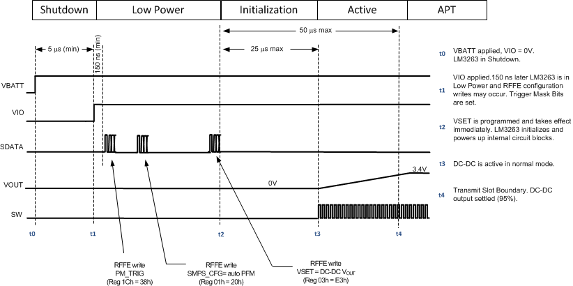 Figure 19. Non-Triggered Start-Up Sequence
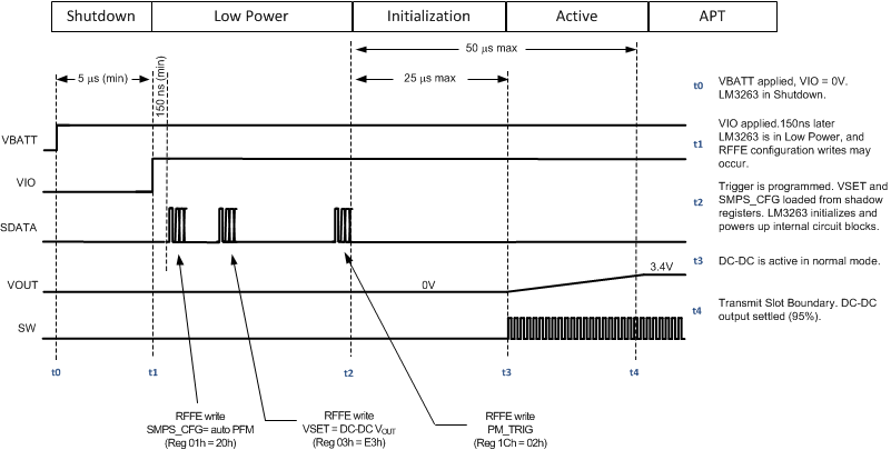 Figure 20. Triggered Start-Up Sequence
7.4 Device Functional Modes
7.4.1 Shutdown Mode
Shutdown mode is entered whenever the voltage on the VIO pin is 0 V. The communications and the controls are not powered. In this mode, the current consumption is 0.02 µA (typical).
7.4.2 Low-Power Mode
Low-power mode is the initial default state when VIO is applied. In this mode, the DC-DC is disabled, and its SW is tri-state. The current consumption is minimized 0.225 µA (typical). This mode can be entered by programming any one of three registers below:
- Register 00h REGISTER_0 [6:0] to 00h;
- Register 03h VSET_CTRL[7:0] to 00h or 01h;
- Register 1Ch PM_TRIG [7:6] to 10b.
7.4.3 Standby Mode
In standby mode, switching is stopped, and the output power FETs are placed are tri-state. The standby mode can be entered by setting PM_TRIG [7:6] and REGISTER_0 or VSET_CTRL registers.
- Register 00h REGISTER_0 [6:0] to 02h;
- Register 03h VSET_CTRL [7:0] to 04h or 05h;
- Register 1Ch PM_TRIG [7:6] to 00b.
7.4.4 Active Mode
The active mode is a DC-DC converter operating mode that allows the device to function, process RFFE commands, and respond to RFFE commands. This mode can be entered by setting register 1Ch PM_TRIG [7:6] to 00b. Once the device is the active Mode, the DC-DC converter operating mode and the output voltage can be programmed by using REGISTER_0 [6:0] and VSET_CTRL[7:0] registers.
7.4.5 User States
7.5 Programming
7.5.1 RFFE Interface
The digital control serial bus interface provides MIPI RF front-end control Interface compatible access to the programmable functions and registers on the device. The LM3263 uses a three-pin digital interface: two for bidirectional communications between the IC’s connected to the bus, along with an interface voltage reference VIO that also acts as asynchronous enable and reset. When VIO voltage supply is applied to the bus, it enables the Slave interface and resets the user-defined Slave registers to the default settings. The LM3263 can be set to shutdown mode via the asynchronous VIO signal or low-power mode by setting the appropriate register via the serial bus interface. The two communication lines are serial data (SDATA), and clock (SCLK). SCLK and SDATA must be held low until VIO is present. The LM3263 connects as slave on a single-master serial bus interface.
The SDATA signal is bidirectional, driven by the Master or a Slave. Data is written on the rising edge (transition from logical level zero to logical level one) of the SCLK signal by both Master and Slaves. Master and Slave both read the data on the falling edge (transition from logical level one to logical level zero) of the SCLK signal. A logic-low level applied to VIO signal powers off the digital interface.
7.5.2 Supported Command Sequences
 Figure 22. Register 0 Write
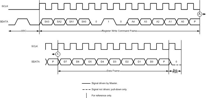 Figure 23. Register Write
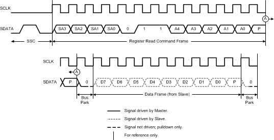 Figure 24. Register Read
7.5.3 Device Enumeration
The interface component recognizes broadcast Slave Address (SID) of 0000b and is configured, via internal interface signals, with a unique SID address (USID) and a group SID address (GSID). The USID is set to 0100b and GSID set to 0000b. The register-set component typically sets the USID to a fixed value; however, it is also possible to select a second pre-set USID if a second LM3263 device is needed on the board. This second User ID can be set by forcing a voltage > 1.36 V at the GPO1 pin for USID = 0101b. Refer to GPO1 for detailed usage and programmability of the USID. The USID can also be re-programmed via the standard protocol for programming the RFFE as defined in the RFFE spec. The USID must not be programmed to the reserved broadcast slave id of 0000b. A value of 0000b is ignored by the device.
7.5.4 GPO1
GPO1 has two functions. The first function is an input to select the default USID, and the second function is to be a general purpose output.
The state of the GPO1 pin at start-up determines the default USID. If the GPO1 pin is low or left floating at start-up, the USID is 0100b. If the GPO1 pin is high at start-up, the USID is 0101b. One method to set the GPO1 pin high is to place a pullup resistor (39 KΩ) on the GPO1 pin.
When the GPO1 pin is used as the general purpose output, GPO_CTRL [6] must be set to 1b. Once it has been enabled as the general purpose output, GPO_CTRL [7] determines the state driven to the GPO1 pin. The pullup resistor must be placed either as an external pullup on the board or through an internal pullup on the general purpose input which is tied to the GPO1 pin.
The GPO1 pin can be left floating if unused.
7.5.5 Trigger Registers
Trigger registers are indicated in the RFFE register map by the Trigger column. All trigger registers are tied to each of the TRIG_0-2 register bits. When a trigger register is written directly across the RFFE interface, the new value is not loaded into the register until one of the TRIG0-2 register bits is written with a 1 and the associated TRIG_MSK_x bit for that TRIG_x is not set. (Triggers are ignored when their associated masking bit is set.) When all 3 TRIG_MSK_0-2 bits are set (all triggers are masked) the trigger feature is disabled, and any trigger registers are loaded directly at the time of the write operation to that register rather than waiting for a trigger event to update.
7.5.6 Control Interface Timing Parameters
 Figure 25. Clock Timing
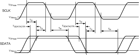 Figure 26. Setup and Hold Timing
| PARAMETER | MIN | TYP | MAX | UNIT | |
|---|---|---|---|---|---|
| TCLK | Clock time period | 38.5 | ns | ||
| TSCLKOH | Clock high time | 11.25 | ns | ||
| TSCLKOL | Clock low time | 11.25 | ns | ||
| TS | Data setup time | 1 | ns | ||
| TH | Data hold time | 5 | ns | ||
| TD-Forward | Time for data output valid from SCLK rising edge | 10.25 | ns | ||
| TD-Reverse | Time for data output valid from SCLK rising edge | 22 | ns | ||
| TSDATAOTR | SDATA output transition (rise/fall) time | 2.1 | 6.5 | ns | |
7.6 Register Map
| Addr | Register Contents | |||||
|---|---|---|---|---|---|---|
| 00h | REGISTER _0 | |||||
| Bits | Function | Default | Trigger* | R/W | Description | |
| 7 | RSVD | 0 | N/A | N/A | Reserved | |
| 6:0 | VSET[7:1] | 00h | Yes | R/W | Register 00h interacts with Register 03h. DC-DC converter mode and output voltage control bits 00h : Low-power mode 01h : Reserved 02h : Standby mode 03h to 7Eh : active mode, setting output voltage is enabled. Output voltage can be set 0.4 V to 3.6 V by 0Dh to 78h with 30-mV steps 7Fh : Forced-bypass mode VSET[7:1] (dec) = Desired VOUT / 0.03 (round up decimals), then converts a decimal number to hexadecimal. |
|
| 01h | SMPS_CFG | |||||
| Bits | Function | Default | Trigger* | R/W | Description | |
| 7:6 | RSVD | 0 | N/A | N/A | Reserved | |
| 5 | MODE | 0 | Yes | R/W | Switching mode select bit 0: Forced-PWM mode (PWM only) 1: Auto-PFM mode (PFM/PWM) |
|
| 4 | BYPS | 0 | Yes | R/W | Forced bypass bit 0: Auto-bypass mode 1: Forced-bypass mode |
|
| 3:0 | RSVD | 0h | N/A | N/A | Reserved | |
| 02h | GPO_CTRL | |||||
| Bits | Function | Default | Trigger* | R/W | Description | |
| 7 | GPO1_OUT | 0 | Yes | R/W | GPO1 output control 0: Low state 1: High state |
|
| 6 | GPO1_MODE | 0 | Yes | R/W | GPO1 Mode Selection 0 : General Purpose Output disabled 1 : General Purpose output driven by GPO1_OUT |
|
| 5:0 | RSVD | 00h | N/A | N/A | Reserved | |
| 03h | VSET_CTRL | |||||
| Bits | Function | Default | Trigger* | R/W | Description | |
| 7:0 | VSET[7:0] | 00h | Yes | R/W | DC-DC converter mode and output voltage fine control bits 00h-01h : Low-power mode 02h-03h : Reserved 04h-05h : Standby mode 06h to FDh : Active mode, setting output voltage is enabled. Output voltage can be set 0.4 V to 3.6 V by 1Bh to F0h with 15-mV steps FEh-FFh : Forced bypass mode VSET[7:0] (dec) = Desired VOUT / 0.015 (round up decimals), then converts a decimal number to hexadecimal. |
|
| 1Ah | RFFE_STATUS | |||||
| Bits | Function | Default | Trigger* | R/W | Description | |
| 7 | SWRESET | 0 | No | Software Reset. A write to 1 causes all registers except for USID to be reset. Always reads back 0. | ||
| 6 | CMD_FRAME_PERR | 0 | No | Set if parity error detected in command frame. Cleared on read. Write has no effect on this bit. | ||
| 5 | CMD_LENGTH_ERR | 0 | No | Error when transaction interrupted by new SSC. Cleared on read. Write has no effect on this bit. | ||
| 4 | RSVD | 0 | No | Reserved | ||
| 3 | DATA_FRAME_PERR | 0 | No | Write data frame parity error. Cleared on read. Write has no effect on this bit. | ||
| 2 | RD_UNUSED_REG | 0 | No | Read command to an invalid register. Cleared on read. Write has no effect on this bit. | ||
| 1 | WR_UNUSED_REG | 0 | No | Write command to an invalid register. Cleared on read. Write has no effect on this bit. | ||
| 0 | BID_GID_ERR | 0 | No | Read command with a broadcast ID or Group ID. Cleared on read. Write has no effect on this bit. | ||
| 1Bh | GROUP_ID | |||||
| Bits | Function | Default | Trigger* | R/W | Description | |
| 7:4 | RSVD | 0h | N/A | N/A | Reserved | |
| 3:0 | GSID | 0h | No | Group slave ID | ||
| 1Ch | PM_TRIG | |||||
| Bits | Function | Default | Trigger* | R/W | Description | |
| 7:6 | PWR_MODE | 10b | No | R/W | Power Mode Bits. 00b = Active mode 01b = Restore default settings 10b = Low-power mode 11b = Reserved |
|
| 5 | TRIG_MSK_2 | 0 | No | Mask bit for Trigger 2. Broadcast write to this bit is ignored. | ||
| 4 | TRIG_MSK_1 | 0 | No | Mask bit for Trigger 1. Broadcast write to this bit is ignored. | ||
| 3 | TRIG_MSK_0 | 0 | No | Mask bit for Trigger 0. Broadcast write to this bit is ignored. | ||
| 2 | TRIG_2 | 0 | No | Write to a 1 loads trigger registers with last written value TRIG_MSK_2 is cleared. Write to 0 has no affect. | ||
| 1 | TRIG_1 | 0 | No | Write to a 1 loads trigger registers with last written value TRIG_MSK_1 is cleared. Write to 0 has no effect. | ||
| 0 | TRIG_0 | 0 | No | Write to a 1 loads trigger registers with last written value TRIG_MSK_0 is cleared. Write to 0 has no effect. | ||
| 1Dh | PRODUCT ID | |||||
| Bits | Function | Default | Trigger* | R/W | Description | |
| 7:0 | PRODUCT_ID | 82h | No | R | Product Identification Bits. Product ID default value cannot be overwritten. | |
| 1Eh | MANUFACTURER ID, LSB | |||||
| Bits | Function | Default | Trigger* | R/W | Description | |
| 7:0 | MANID[7:0] | 02h | No | R | Manufacturer Identification, bits 7:0. Manufacturer ID default value cannot be overwritten. | |
| 1Fh | MANUFACTURER ID, MSB | |||||
| Bits | Function | Default | Trigger* | R/W | Description | |
| 7:6 | RSVD | 00b | N/A | N/A | Reserved | |
| 5:4 | MANID[5:4] | 01b | No | R | Manufacturer Identification, bits 5:4. Manufacturer ID default value cannot be overwritten. | |
| 3:0 | USID | 010xb | No | Unique Slave Identifier. Bit 0 (x) of USID is tied to the state of the GPO1 pin. 0100b: GPO1= Low state or floating 0101b: GPO1= High state |
||
* Trigger = Yes: When all PM_TRIG.TRIG_MSK_* bits are set 1, REGISTER_0 is written immediately during a write operation. If any PM_TRIG.TRIG_MSK_* bits are cleared (0), REGISTER_0 is not updated to the new value after a write operation only after an unmasked PM_TRIG.TRIG_* bit is subsequently written to a 1.