SNVS837B June 2013 – April 2016 LM3263
PRODUCTION DATA.
- 1 Features
- 2 Applications
- 3 Description
- 4 Revision History
- 5 Pin Configuration and Functions
- 6 Specifications
-
7 Detailed Description
- 7.1 Overview
- 7.2 Functional Block Diagram
- 7.3
Feature Description
- 7.3.1 PWM Operation
- 7.3.2 PFM Operation
- 7.3.3 Active Current Assist and Analog Bypass (ACB)
- 7.3.4 Bypass Operation
- 7.3.5 Dynamic Adjustment of Output Voltage
- 7.3.6 DC-DC Operating Mode Selection
- 7.3.7 Internal Synchronous Rectification
- 7.3.8 Current Limit
- 7.3.9 Timed Current Limit
- 7.3.10 Thermal Overload Protection
- 7.3.11 Start-Up
- 7.4 Device Functional Modes
- 7.5 Programming
- 7.6 Register Map
- 8 Application Information
- 9 Power Supply Recommendations
- 10Layout Considerations
- 11Device and Documentation Support
- 12Mechanical, Packaging, and Orderable Information
6 Specifications
6.1 Absolute Maximum Ratings
over operating free-air temperature range (unless otherwise noted)(1)(2)| MIN | MAX | UNIT | ||
|---|---|---|---|---|
| VBATT pins to GND (PVIN, SVDD, PACB to PGND, SGND, BGND) | –0.2 | 6 | V | |
| FB, SW, GPO1, ACB, VIO, SDATA, SCLK | GND – 0.2 V | See(3) | V | |
| Continuous power dissipation(4) | Internally limited | |||
| Maximum operating junction temperature, TJ-MAX | 150 | °C | ||
| Maximum lead temperature (soldering 10 seconds) | 260 | °C | ||
| Storage temperature, Tstg | −65 | 150 | °C | |
(1) Stresses beyond those listed under Absolute Maximum Ratings may cause permanent damage to the device. These are stress ratings only, which do not imply functional operation of the device at these or any other conditions beyond those indicated under Recommended Operating Conditions. Exposure to absolute-maximum-rated conditions for extended periods may affect device reliability.
(2) All voltages are with respect to the potential at the GND pins.
(3) Abs Max for FB, SW, GPO1, ACB, VIO, SDATA, SCLK is the lessor of VIN + 0.2 V, or 6 V.
(4) Internal thermal shutdown circuitry protects the device from permanent damage. Thermal shutdown engages at TJ = 150°C (typical) and disengages at TJ = 125°C (typical).
6.2 ESD Ratings
| VALUE | UNIT | |||
|---|---|---|---|---|
| V(ESD) | Electrostatic discharge | Human-body model (HBM), per ANSI/ESDA/JEDEC JS-001(1) | ±1000 | V |
| Charged-device model (CDM), per JEDEC specification JESD22-C101(2) | ±250 | |||
(1) JEDEC document JEP155 states that 500-V HBM allows safe manufacturing with a standard ESD control process.
(2) JEDEC document JEP157 states that 250-V CDM allows safe manufacturing with a standard ESD control process.
6.3 Recommended Operating Conditions
over operating free-air temperature range (unless otherwise noted)| MIN | MAX | UNIT | ||
|---|---|---|---|---|
| Input voltage range PVIN, SVDD, PACB | 2.7 | 5.5 | V | |
| Input voltage range VIO | 1.65 | 1.95 | V | |
| Recommended current load | 0 | 2.5 | A | |
| Junction temperature, TJ | –30 | 125 | °C | |
| Ambient temperature, TA(1) | –30 | 90 | °C | |
(1) In applications where high power dissipation and/or poor package thermal resistance is present, the maximum ambient temperature may have to be de-rated. Maximum ambient temperature (TA-MAX) is dependent on the maximum operating junction temperature (TJ-MAX-OP = 125°C), the maximum power dissipation of the device in the application (PD-MAX), and the junction-to ambient thermal resistance of the part/package in the application (RθJA), as given by the following equation: TA-MAX = TJ-MAX-OP – (RθJA × PD-MAX). At higher power levels duty cycle usage is assumed to drop (that is, maximum power 12.5% usage is assumed) for GSM/GPRS mode.
6.4 Thermal Information
| THERMAL METRIC(1) | LM3263 | UNIT | |
|---|---|---|---|
| YFQ (DSBGA) | |||
| 16 PINS | |||
| RθJA | Junction-to-ambient thermal resistance | 77.1 | °C/W |
| RθJC(top) | Junction-to-case (top) thermal resistance | 0.4 | °C/W |
| RθJB | Junction-to-board thermal resistance | 15.4 | °C/W |
| ψJT | Junction-to-top characterization parameter | 2.0 | °C/W |
| ψJB | Junction-to-board characterization parameter | 15.1 | °C/W |
(1) For more information about traditional and new thermal metrics, see the Semiconductor and IC Package Thermal Metrics application report, SPRA953.
6.5 Electrical Characteristics
Unless otherwise noted, all limits apply to the Typical Application with VBATT = 3.8 V (= PVIN = SVDD = PACB), VIO = 1.8 V, TJ = 25°C.(1)(2)(3)| PARAMETER | TEST CONDITIONS | MIN | TYP | MAX | UNIT | |
|---|---|---|---|---|---|---|
| VFB,MIN | Feedback voltage at minimum setting | VSET[7:0] = 1Bh, SMPS_CFG[5] = 1b | 0.4 | V | ||
| VSET[7:0] = 1Bh, SMPS_CFG[5] = 1b −30°C ≤ TJ = TA ≤ 90°C |
0.35 | 0.45 | ||||
| VFB,MAX | Feedback voltage at maximum setting | VSET[7:0] = F0h, VBATT = 3.9 V, SMPS_CFG[5] = 0b | 3.6 | V | ||
| VSET[7:0] = F0h, VBATT = 3.9 V, SMPS_CFG[5] = 0b −30°C ≤ TJ = TA ≤ 90°C |
3.492 | 3.708 | ||||
| ISHDN | Shutdown supply current | SW = 0 V, VIO = 0 V(4) | 0.02 | µA | ||
| SW = 0 V, VIO = 0 V(4)
−30°C ≤ TJ = TA ≤ 90°C |
4 | |||||
| IL-PWR | Low-power mode supply current | VSET[7:0] = 00h | 0.225 | µA | ||
| IQ-PFM | PFM mode supply current into SVDD | No switching(5), SMPS_CFG[5] = 1b | 360 | µA | ||
| No switching(5), SMPS_CFG[5] = 1b −30°C ≤ TJ = TA ≤ 90°C |
425 | |||||
| IQ PWM | PWM mode supply current | No switching(5), SMPS_CFG[5] = 0b | 1240 | µA | ||
| No switching(5), SMPS_CFG[5] = 0b −30°C ≤ TJ = TA ≤ 90°C |
1400 | |||||
| ILIM, PFET Transient | Positive transient peak current limit | VSET[7:0] = 64h(6) | 1.9 | A | ||
| VSET[7:0] = 64h(6)
−30°C ≤ TJ = TA ≤ 90°C |
2.1 | |||||
| ILIM, PFET Steady-State | Positive steady-state peak current limit | VSET[7:0] = 64h(6) | 1.45 | A | ||
| VSET[7:0] = 64h(6)
−30°C ≤ TJ = TA ≤ 90°C |
1.35 | 1.65 | ||||
| ILIM, P-ACB | Positive active current assist peak current limit | VSET[7:0] = 64h(6) | 1.7 | A | ||
| VSET[7:0] = 64h(6)
−30°C ≤ TJ = TA ≤ 90°C |
1.4 | 2 | ||||
| ILIM,NFET | NFET current limit | VSET[7:0] = A7h(6) | −1.5 | A | ||
| ƒOSC | Average Internal oscillator frequency | VSET[7:0] = A7h | 2.7 | MHz | ||
| VSET[7:0] = A7h −30°C ≤ TJ = TA ≤ 90°C |
2.43 | 2.97 | ||||
| IVIO-IN | VIO voltage average input current | Average during a 26-MHz write | 1.25 | mA | ||
| VIORST | RFFE I/O voltage reset voltage | VIO toggled low | 0.45 | V | ||
| IINVIO | VIO reset current | VIO = 0.45 V | −1 | 1 | µA | |
| IIN | SDATA, SCLK input current | VIO = 1.95 V | −1 | 1 | µA | |
| VIH | Input high-level threshold SDATA, SCLK | 0.4 × VIO | 0.7 × VIO | V | ||
| VIL | Input low-level threshold SDATA, SCLK | 0.3 × VIO | 0.6 × VIO | V | ||
| VIH-GPO | Input high-level threshold GPO1 | −30°C ≤ TJ = TA ≤ 90°C | 1.35 | V | ||
| VIL-GPO | Input low-level threshold GPO1 | −30°C ≤ TJ = TA ≤ 90°C | 0.67 | V | ||
| VOH | Output high-level threshold SDATA | ISDATA = 2 mA | VIO × 0.8 | VIO + 0.01 | V | |
| VOL | Output low-level threshold SDATA | ISDATA = –2 mA | VIO × 0.2 | V | ||
| VOH-GPO | Output high-level threshold GPO | IOUT = ±200 µA | VIO – 0.15 | VIO + 0.1 | V | |
| VOL-GPO | Output low-level threshold GPO | –0.4 | 0.3 | V | ||
| VSET-LSB | Output voltage LSB | VSET[7:0] = A7h to A8h | 15 | mV | ||
(1) All voltages are with respect to the potential at the GND pins.
(2) Minimum and Maximum limits are specified by design, test, or statistical analysis.
(3) The parameters in Electrical Characteristics are tested under open loop conditions at PVIN = SVDD = PACB = 3.8 V.
(4) Shutdown current includes leakage current of PFET.
(5) IQ specified here is when the part is not switching.
(6) Current limit is built-in, fixed, and not adjustable.
6.6 System Characteristics
The following spec table entries are specified by design and verifications providing the component values in the Typical Application are used (L = 1.5 µH, DCR = 120 mΩ, TOKO DFE201610MT-1R5N, CIN = 10 µF, 6.3 V, 0402, Samsung CL05A106MP5NUN, COUT = 10 µF + 4.7 µF + 3 × 1 µF; 10 V, 0402, Samsung CL05A106MP5NUN, CL05A475MPNRN; 6.3 V, 0201, TDK, C0603X5R0J105M). These parameters are not verified by production testing. Minimum and maximum values are specified over the ambient temperature range TA = –30°C to +90°C. Typical values are specified at VBATT = 3.8 V (= PVIN = SVDD = PACB), VIO = 1.8 V, SMPS_CFG = 20h, and TA = 25°C, unless otherwise stated.| PARAMETER | TEST CONDITIONS | MIN | TYP | MAX | UNIT | |
|---|---|---|---|---|---|---|
| TON | Turnon time (time for output to reach 95% of 3.4-V value from the end of the SCLK pulse) | VBATT = 4.2 V, VSET[7:0] =00h to E3h, VSET = 3.4 V, IOUT ≤ 1 mA | 50 | µs | ||
| TRESPONSE | Time for VOUT to rise from 0.09 V to 3.4 V (3.07 V, 90% of delta VOUT from the end of SCLK pulse) | VBATT = 3.8 V, RLOAD = 68 Ω VSET[7:0] = 06h to E3h SMPS_CFG[5] = 0b/1b |
15 | µs | ||
| Time for VOUT to fall from 3.4 V to 0.09 V (0.42 V, 10% of delta VOUT from the end of SCLK pulse) | VBATT = 3.8 V, RLOAD = 68 Ω VSET[7:0] = E3h to 06h SMPS_CFG[5] = 0b/1b |
15 | ||||
| Time for VOUT to rise from 0.8 V to 3.3 V (3.05V, 90% of delta VOUT from the end of SCLK pulse) | VBATT = 3.8 V, RLOAD = 20 Ω VSET[7:0] =36h to DCh |
7.4 | 12 | |||
| Time for VOUT to fall from 3.3 V to 0.8 V (1.05 V, 10% of delta VOUT from the end of SCLK pulse) | VBATT = 3.8 V, RLOAD = 20 Ω VSET[7:0] = DCh to 36h |
6.8 | 12 | |||
| Time for VOUT to rise from 1.4 V to 3.4 V (3.2 V, 90% of delta VOUT from the end of SCLK pulse) | VBATT = 3.8 V, RLOAD = 6.8 Ω VSET[7:0] = 5Eh to E3h |
10 | ||||
| Time for VOUT to fall from 3.4 V to 1.4 V (1.6 V, 10% of delta VOUT from the end of SCLK pulse) | VBATT = 3.8 V, RLOAD = 6.8 Ω VSET[7:0] = E3h to 5Eh |
10 | ||||
| Time for VOUT to rise from 1.8 V to 2.8 V (2.7 V, 90% of delta VOUT from the end of SCLK pulse) | VBATT = 3.8 V, RLOAD = 2.2 Ω VSET[7:0] = 78h to BBh SMPS_CFG[5] = 0b |
15 | ||||
| Time for VOUT to fall from 2.8 V to 1.8 V (1.9 V, 10% of delta VOUT from the end of SCLK pulse) | VBATT = 3.8 V, RLOAD = 2.2 Ω VSET[7:0] = BBh to 78h SMPS_CFG[5] = 0b |
15 | ||||
| TBypass | Time for VSET to rise from 0.09V to PVIN after BYPASS transition (90%) | VBATT = 3.6 V, IOUT ≤ 1 mA, VSET[7:0] = 06h to FFh |
20 | µs | ||
| Rtot-drop | Total dropout resistance in bypass mode | VSET[7:0] = FAh, Max value at VBATT = 3.1 V, Inductor DCR ≤ 151 mΩ | 45 | 55 | mΩ | |
| IOUT | Maximum load current in PWM mode | Switcher + ACB | 2.5 | A | ||
| IOUT, PU | Maximum output transient pullup current limit | Switcher + ACB(6) | 3 | |||
| IOUT, PD, PWM | PWM maximum output transient pulldown current limit | Switcher + ACB(6) | −3 | |||
| IOUT, MAX_PFM | Maximum output load current in PFM mode | VBATT = 3.8 V, VSET = 3.2 V | 60 | mA | ||
| Linearity | Linearity in control range of VSET = 0.4 V to 3.6 V | VBATT = 3.9 V(2), Monotonic in nature; VSET[7:0] = 1Bh to F0h, SMPS_CFG[5] = 0b |
–3% | 3% | ||
| –50 | 50 | mV | ||||
| η | Efficiency | VBATT = 3.8 V, VSET= 0.5 V, IOUT = 5mA |
52% | 56% | ||
| VBATT = 3.8 V, VSET= 1.8 V, IOUT = 10 mA |
78% | 82% | ||||
| VBATT = 3.8 V, VSET= 1.6 V, IOUT = 130 mA |
83% | 89% | ||||
| VBATT = 3.8 V, VSET = 2.5 V, IOUT = 250 mA |
90% | 94% | ||||
| VBATT = 3.8 V, VSET = 3.4 V, IOUT = 550 mA |
93% | 95% | ||||
| VBATT = 3.8 V, VSET = 1 V, IOUT = 400 mA, SMPS_CFG[5] = 0b |
81% | 85% | ||||
| VBATT = 3.8 V, VSET = 3.5 V, IOUT = 1900 mA, SMPS_CFG[5] = 0b |
89% | 92% | ||||
| VRIPPLE | 2.7-MHz PWM normal operation ripple | VBATT = 3.2 V to 4.3 V, VSET = 0.4 V to 3.6 V, RLOAD = 1.9 Ω(1)
SMPS_CFG[5]= 0b |
1 | 3 | mVpp | |
| Ripple voltage at pulse skipping condition | VBATT = 3.2 V, VSET = 3 V, RLOAD = 1.9 Ω (1) SMPS_CFG[5]= 0b |
8 | ||||
| PFM ripple voltage | VBATT = 3.2 V, VSET = 3 V, IOUT = 40 mA |
50 | ||||
| VBATT = 3.2 V, VSET = 2.5 V, IOUT = 10 mA |
50 | |||||
| VBATT = 3.2 V, VSET< 0.5 V, IOUT = 5 mA |
50 | |||||
| Line_tr | Line transient response | VBATT = 3.6 V to 4.2 V, TR = TF = 10 µs, VSET = 3.2 V, IOUT = 500 mA |
50 | mVpk | ||
| Load_tr | Load transient response | VSET = 3 V, TR = TF = 10 µs, IOUT = 0 A to 1.2 A, SMPS_CFG[5] = 0b |
60 | mVpk | ||
| Max Duty Cycle | Maximum duty cycle | 100% | ||||
| PFM_Freq | Minimum PFM frequency | VBATT = 3.2 V, VSET = 1 V, IOUT = 10 mA |
100 | 160 | KHz | |
| VBATT = 3.2 V, VSET = 0.5 V, IOUT = 5 mA |
34 | 55 | ||||
| NSET | VSET DAC number of bits | Monotonic | 8 | Bits | ||
| TSETUP | Power-up time (time for RFFE bus active after VIO applied) | VIO = Low to 1.65 V | 50 | ns | ||
| TVIO-RST | VIO supply reset timing | VIO = 0.45 V | 10 | µs | ||
(1) Ripple voltage must be measured at COUT electrode on a well-designed PC board using suggested inductor and capacitors.
(2) Linearity limits are ±3% or ±50 mV whichever is larger.
6.7 Typical Characteristics
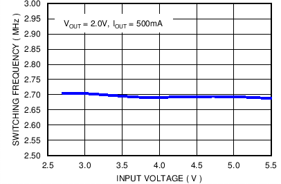
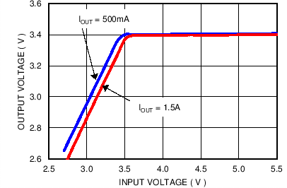
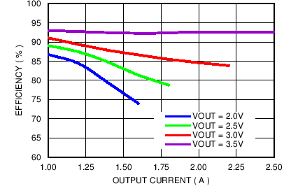
VBATT = 3.8 V, TA = 25°C, unless otherwise noted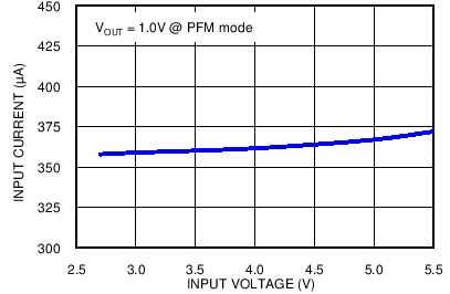
| No load |
| VOUT = 3.4 V |

| Auto-PFM Mode | IOUT = 150 mA to 750 mA | |
| Forced PWM Mode | IOUT = 1 A to 2.5 A |

| Forced PWM | VOUT = 1.4 V to 3.4 V | RLOAD = 1.9 Ω |
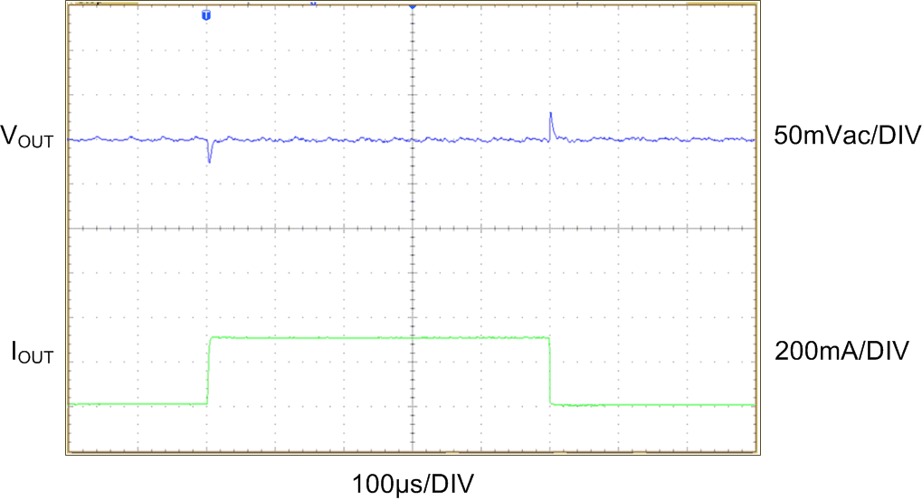
| VOUT = 2.5 V | IOUT= 0 mA to 300 mA | |

| VBATT = 4.2 V | VOUT = 3 V | IOUT= 0 mA to 1.2 A |
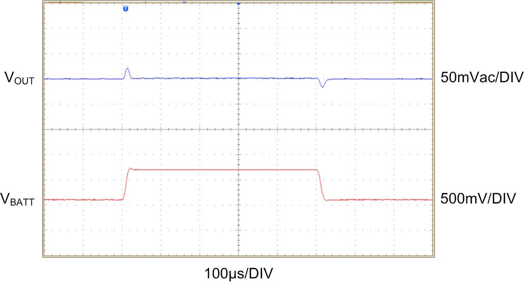
| VBATT = 3.6 V to 4.2 V | VOUT = 1 V | RLOAD = 6.8 Ω |
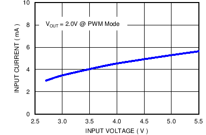
| No load |


| Auto-PFM Mode | IOUT = 10 mA to 150 mA |

| Forced PWM Mode | IOUT = 100 mA to 1000 mA |
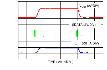
| Auto PFM | VOUT = 0.4 V to 3.4 V | RLOAD = 6.8 Ω |

| PFM Mode | VOUT = 1 V | IOUT= 0 mA to 60 mA |

| VOUT = 3 V | IOUT= 0 mA to 700 mA | |

| VBATT = 3.6 V to 4.2 V | VOUT = 2.5 V | RLOAD = 6.8 Ω |

| VBATT = 4.2 V | VOUT = 2.5 V | RLOAD = 6.8 Ω to 0 Ω |