SNVS853E August   2012  – August 2018 LMZ21701

PRODUCTION DATA.  

  1. Features
  2. Applications
  3. Description
    1.     Device Images
      1.      Simplified Schematic
      2.      Efficiency for VIN = 12 V
  4. Revision History
  5. Pin Configuration and Functions
    1.     Pin Functions
  6. Specifications
    1. 6.1 Absolute Maximum Ratings
    2. 6.2 ESD Ratings
    3. 6.3 Recommended Operating Conditions
    4. 6.4 Thermal Information
    5. 6.5 Electrical Characteristics
    6. 6.6 Typical Characteristics
  7. Detailed Description
    1. 7.1 Overview
    2. 7.2 Functional Block Diagram
    3. 7.3 Package Construction
    4. 7.4 Feature Description
      1. 7.4.1 Input Undervoltage Lockout
      2. 7.4.2 Enable Input (EN)
      3. 7.4.3 Soft Start and Tracking Function (SS)
      4. 7.4.4 Power Good Function (PG)
      5. 7.4.5 Output Voltage Setting
      6. 7.4.6 Output Current Limit and Output Short Circuit Protection
      7. 7.4.7 Thermal Protection
    5. 7.5 Device Functional Modes
      1. 7.5.1 PWM Mode Operation
      2. 7.5.2 PSM Operation
  8. Application and Implementation
    1. 8.1 Application Information
    2. 8.2 Typical Application
      1. 8.2.1 Design Requirements
      2. 8.2.2 Detailed Design Procedure
        1. 8.2.2.1 Custom Design With WEBENCH® Tools
        2. 8.2.2.2 Input Capacitor (CIN)
        3. 8.2.2.3 Output Capacitor (COUT)
        4. 8.2.2.4 Soft-start Capacitor (CSS)
        5. 8.2.2.5 Power Good Resistor (RPG)
        6. 8.2.2.6 Feedback Resistors (RFBB and RFBT)
      3. 8.2.3 Application Curves
        1. 8.2.3.1 VOUT = 1.2 V
        2. 8.2.3.2 VOUT = 1.8 V
        3. 8.2.3.3 VOUT = 2.5 V
        4. 8.2.3.4 VOUT = 3.3 V
        5. 8.2.3.5 VOUT = 5.0 V
    3. 8.3 Do's and Don'ts
  9. Power Supply Recommendations
    1. 9.1 Voltage Range
    2. 9.2 Current Capability
    3. 9.3 Input Connection
      1. 9.3.1 Voltage Drops
      2. 9.3.2 Stability
  10. 10Layout
    1. 10.1 Layout Guidelines
      1. 10.1.1 Minimize the High di/dt Loop Area
      2. 10.1.2 Protect the Sensitive Nodes in the Circuit
      3. 10.1.3 Provide Thermal Path and Shielding
    2. 10.2 Layout Example
      1. 10.2.1 High Density Layout Example for Space Constrained Applications
        1. 10.2.1.1 35 mm² Solution Size (Single Sided)
  11. 11Device and Documentation Support
    1. 11.1 Device Support
      1. 11.1.1 Development Support
        1. 11.1.1.1 Custom Design With WEBENCH® Tools
    2. 11.2 Trademarks
    3. 11.3 Electrostatic Discharge Caution
    4. 11.4 Glossary
  12. 12Mechanical, Packaging, and Orderable Information
    1. 12.1 Tape and Reel Information

VOUT = 2.5 V

LMZ21701 TYP_SCH.gifFigure 44. Typical Applications Circuit
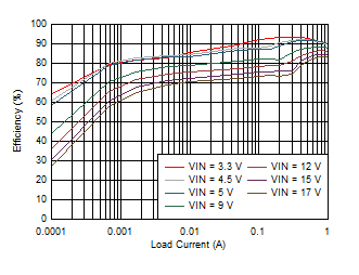
LMZ21701 D017_LMZ21701_25C_2.5VOUT_EFFICIENCY_LOG_SNVS853.gifFigure 46. Efficiency VOUT = 2.5 V
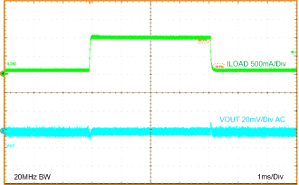
LMZ21701 LMZ21701_2.5VOUT_LOAD_TRANS_100mA_to_1000mA_snvs853.gifFigure 48. Load Transient VOUT = 2.5 V
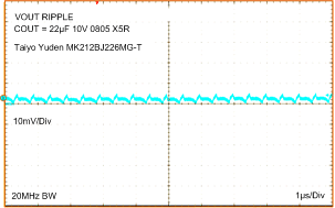
LMZ21701 LMZ21701_2.5VOUT_RIPPLE_20MHzBW_snvs853.gifFigure 50. 20MHz Oscilloscope Bandwidth
Output Voltage Ripple VOUT = 2.5 V
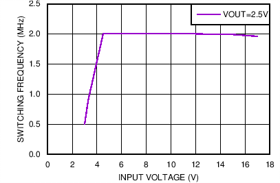
LMZ21701 LMZ21701_FSW_2.5VOUT_snvs853.pngFigure 52. Typical Switching Frequency at 1000 mA Load VOUT = 2.5 V
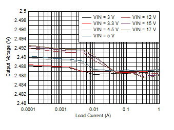
LMZ21701 D018_LMZ21701_25C_2.5VOUT_LINE_AND_LOAD_REG_LOG_SNVS853.gifFigure 54. Line and Load Regulation VOUT = 2.5 V
LMZ21701 2.5V_BOM_snvs853.gifFigure 45. External Component Values
(VOUT = 2.5 V)
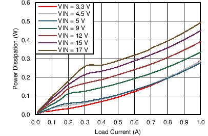
LMZ21701 LMZ21701_25C_2.5VOUT_POWER_DISSIPATION_snvs853.pngFigure 47. Power Dissipation VOUT = 2.5 V
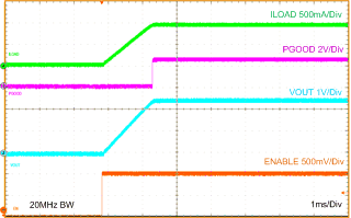
LMZ21701 LMZ21701_2.5VOUT_STARTUP_snvs853.gifFigure 49. Startup VOUT = 2.5 V
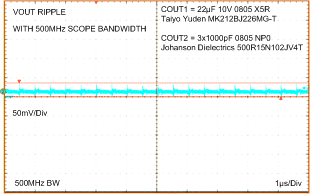
LMZ21701 LMZ21701_2.5VOUT_RIPPLE_500MHzBW_snvs853.gifFigure 51. 500 MHz Oscilloscope Bandwidth, 3x1000 pF additional output capacitance
Output Voltage Ripple and HF Noise VOUT = 2.5 V
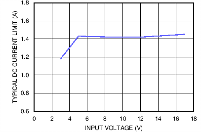
LMZ21701 LMZ21701_ICL_2.5V_85C_snvs853.pngFigure 53. Typical Current Limit VOUT = 2.5 V, TA = 85 °C
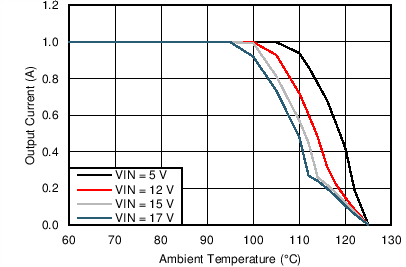
LMZ21701 LMZ21701SIL_2.5VO_47CperW_snvs853.pngFigure 55. Thermal Derating for θJA = 47 ºC/W, VOUT = 2.5 V