SNVS896B August 2013 – November 2014 LM27403
PRODUCTION DATA.
- 1 Features
- 2 Applications
- 3 Description
- 4 Revision History
- 5 Description (Continued)
- 6 Pin Configuration and Functions
- 7 Specifications
-
8 Detailed Description
- 8.1 Overview
- 8.2 Functional Block Diagram
- 8.3
Feature Description
- 8.3.1 Input Range: VIN
- 8.3.2 Output Voltage: FB Voltage and Accuracy
- 8.3.3 Input and Bias Rail Voltages: VIN and VDD
- 8.3.4 Precision Enable: UVLO/EN
- 8.3.5 Switching Frequency
- 8.3.6 Temperature Sensing: D+ and D-
- 8.3.7 Thermal Shutdown: OTP
- 8.3.8 Inductor-DCR-Based Overcurrent Protection
- 8.3.9 Current Sensing: CS+ and CS-
- 8.3.10 Current Limit Handling
- 8.3.11 Soft-Start: SS/TRACK
- 8.3.12 Monotonic Startup
- 8.3.13 Prebias Startup
- 8.3.14 Voltage-Mode Control
- 8.3.15 Output Voltage Remote Sense: RS
- 8.3.16 Power Good: PGOOD
- 8.3.17 Gate Drivers: LG and HG
- 8.3.18 Sink and Source Capability
- 8.4 Device Functional Modes
-
9 Application and Implementation
- 9.1 Application Information
- 9.2
Typical Applications
- 9.2.1 Design 1 - High-Efficiency Synchronous Buck Regulator for Telecom Power
- 9.2.2 Design 2 - Powering FPGAs Using Flexible 30A Regulator With Small Footprint
- 9.2.3 Design 3 - Powering Multicore DSPs
- 9.2.4 Design 4 - Regulated 12-V Rail with LDO Low-Noise Auxiliary Output for RF Power
- 9.2.5 Design 5 - High Power Density Implementation From 3.3-V or 5-V Supply Rail
- 10Power Supply Recommendations
- 11Layout
- 12Device and Documentation Support
- 13Mechanical, Packaging, and Orderable Information
1 Features
- Up to 97% Efficiency and 93% Duty Cycle
- Wide Input Voltage Range of 3 V to 20 V
- Switching Frequency From 200 kHz to 1.2 MHz
- Inductor-DCR-Based Overcurrent Protection With Thermal Compensation
- 0.6-V Reference With 1% Feedback Accuracy
- 30-ns Min On-Time for Low VOUT
- Integrated High-Current MOSFET Drivers
- Adaptive Deadtime Control
- Ultrafast Line and Load Transient Response
- High GBW Error Amplifier
- PWM Line Feedforward
- Integrated VDD Bias Supply LDO Subregulator
- Programmable System-Level OTP
- Precision Enable With Hysteresis
- Frequency Synchronization
- Monotonic Prebiased Start-up
- Programmable Soft-Start With Tracking
- Output Remote Sense
- Open-Drain Power Good Indicator
- 4-mm x 4-mm WQFN-24 PowerPAD™ Package
2 Applications
- DC-DC Converters and POL Modules
- Telecommunications Infrastructure
- Embedded Computing, Servers, Storage
3 Description
The LM27403 is a feature-rich, easy-to-use, synchronous buck controller offering exceptional levels of integration and performance for superior efficiency in high power density, point-of-load (POL) DC-DC regulator solutions. The resistor-programmable switching frequency from 200 kHz to 1.2 MHz and integrated, high-current MOSFET gate drivers with adaptive deadtime offer flexibility to optimize solution size and maximize conversion efficiency.
High precision and low output voltage are easily obtained with a 0.6-V, 1% accurate voltage reference together with a 30-ns high-side MOSFET minimum controllable on-time. Using lossless inductor dc resistance (DCR) current sensing and an inexpensive 2N3904 BJT to sense temperature remotely at the inductor, the LM27403 supports accurate and thermally compensated overcurrent protection (OCP).
Device Information(1)
| PART NUMBER | PACKAGE | BODY SIZE (NOM) |
|---|---|---|
| LM27403 | WQFN (24) | 4.00 mm x 4.00 mm |
- For all available packages, see the orderable addendum at the end of the datasheet.
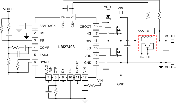
Typical Application Diagram
