-
LM5122 Wide-Input Synchronous Boost Controller With Multiple Phase Capability
- 1 Features
- 2 Applications
- 3 Description
- 4 Revision History
- 5 Pin Configuration and Functions
- 6 Specifications
-
7 Detailed Description
- 7.1 Overview
- 7.2 Functional Block Diagram
- 7.3
Feature Description
- 7.3.1 Undervoltage Lockout (UVLO)
- 7.3.2 High Voltage VCC Regulator
- 7.3.3 Oscillator
- 7.3.4 Slope Compensation
- 7.3.5 Error Amplifier
- 7.3.6 PWM Comparator
- 7.3.7 Soft-Start
- 7.3.8 HO and LO Drivers
- 7.3.9 Bypass Operation (VOUT = VIN)
- 7.3.10 Cycle-by-Cycle Current Limit
- 7.3.11 Clock Synchronization
- 7.3.12 Maximum Duty Cycle
- 7.3.13 Thermal Protection
- 7.4 Device Functional Modes
-
8 Application and Implementation
- 8.1
Application Information
- 8.1.1 Feedback Compensation
- 8.1.2 Sub-Harmonic Oscillation
- 8.1.3 Interleaved Boost Configuration
- 8.1.4 DCR Sensing
- 8.1.5 Output Overvoltage Protection
- 8.1.6 SEPIC Converter Simplified Schematic
- 8.1.7 Non-Isolated Synchronous Flyback Converter Simplified Schematic
- 8.1.8 Negative to Positive Conversion
- 8.2
Typical Application
- 8.2.1 Design Requirements
- 8.2.2
Detailed Design Procedure
- 8.2.2.1 Custom Design With WEBENCH® Tools
- 8.2.2.2 Timing Resistor RT
- 8.2.2.3 UVLO Divider RUV2, RUV1
- 8.2.2.4 Input Inductor LIN
- 8.2.2.5 Current Sense Resistor RS
- 8.2.2.6 Current Sense Filter RCSFP, RCSFN, CCS
- 8.2.2.7 Slope Compensation Resistor RSLOPE
- 8.2.2.8 Output Capacitor COUT
- 8.2.2.9 Input Capacitor CIN
- 8.2.2.10 VIN Filter RVIN, CVIN
- 8.2.2.11 Bootstrap Capacitor CBST and Boost Diode DBST
- 8.2.2.12 VCC Capacitor CVCC
- 8.2.2.13 Output Voltage Divider RFB1, RFB2
- 8.2.2.14 Soft-Start Capacitor CSS
- 8.2.2.15 Restart Capacitor CRES
- 8.2.2.16 Low-Side Power Switch QL
- 8.2.2.17 High-Side Power Switch QH and Additional Parallel Schottky Diode
- 8.2.2.18 Snubber Components
- 8.2.2.19 Loop Compensation Components CCOMP, RCOMP, CHF
- 8.2.3 Application Curves
- 8.1
Application Information
- 9 Power Supply Recommendations
- 10Layout
- 11Device and Documentation Support
- 12Mechanical, Packaging, and Orderable Information
- IMPORTANT NOTICE
LM5122 Wide-Input Synchronous Boost Controller With Multiple Phase Capability
1 Features
- Maximum Input Voltage: 65 V
- Minimum Input Voltage: 3 V (4.5 V for Start-Up)
- Output Voltage up to 100 V
- Bypass (VOUT = VIN) Operation
- 1.2-V Reference with ±1% Accuracy
- Free-Run and Synchronizable Switching to 1 MHz
- Peak-Current-Mode Control
- Robust 3-A Integrated Gate Drivers
- Adaptive Dead-Time Control
- Optional Diode-Emulation Mode
- Programmable Cycle-by-Cycle Current Limit
- Hiccup-Mode Overload Protection
- Programmable Line UVLO
- Programmable Soft Start
- Thermal Shutdown Protection
- Low Shutdown Quiescent Current: 9 μA
- Programmable Slope Compensation
- Programmable Skip-Cycle Mode Reduces Standby Power
- Allows External VCC Supply
- Inductor DCR Current Sensing Capability
- Multi-phase Capability
- Thermally Enhanced 20 or 24-Pin HTSSOP
- Create a Custom Design Using the LM5122 With the WEBENCH® Power Designer
2 Applications
- 12-V, 24-V, and 48-V Power Systems
- Automotive Start-Stop
- Audio Power Supply
- High-Current Boost Power Supply
3 Description
The LM5122 is a multi-phase capable synchronous boost controller intended for high-efficiency synchronous boost regulator applications. The control method is based upon peak-current-mode control. Current-mode control provides inherent line feed forward, cycle-by-cycle current limiting, and ease of loop compensation.
The switching frequency is programmable up to 1 MHz. Higher efficiency is achieved by two robust N-channel MOSFET gate drivers with adaptive dead-time control. A user-selectable diode-emulation mode also enables discontinuous-mode operation for improved efficiency at light load conditions.
An internal charge pump allows 100% duty cycle for high-side synchronous switch (bypass operation). A 180° phase shifted clock output enables easy multi-phase interleaved configuration. Additional features include thermal shutdown, frequency synchronization, hiccup-mode current limit, and adjustable line undervoltage lockout.
Device Information(1)
| PART NUMBER | PACKAGE | BODY SIZE (NOM) |
|---|---|---|
| LM5122 | HTSSOP (20) | 6.50 mm × 4.40 mm |
| LM5122Z | HTSSOP (24) | 7.80 mm × 4.40 mm |
space
space
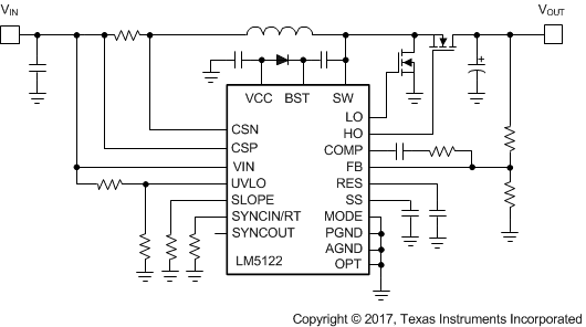
Simplified Application Diagram

4 Revision History
Changes from May 1, 2017 to June 9, 2017
- Changed by splitting out the automotive datasheet from this commercial datasheet Go
- Added 24-pin HTTSOP package optionGo
- Added links for WEBENCH Go
- Added 24-HTSSOP pin configurationGo
- Added 24-HTSSOP Functions Go
- Changed UVLO valueGo
- Changed VCC value Go
- Changed one NC value Go
- Changed from outlet to contact Go
- Added LM5122Z part number Go
- Changed 20-HTSSOP Thermal Information and added 24-HTSSOP thermal valuesGo
- Added ICSP –ICSN (LM5122Z only) specsGo
- Added No load, 50% to 50% (LM5122Z only) specsGo
- Added 24-pin HTSSOPGo
- Added Negative to Positive conversion exampleGo
Changes from F Revision (May 2015) to G Revision
Changes from E Revision (December 2014) to F Revision
- Changed Handling Ratings to ESD Ratings and moved Storage temperature to Absolute Max Ratings Go
- Added Ohm symbol in Current Sense Resistor RS equation 28Go
- Changed typo to reflect an Ohm symbol in Current Sense Resistor RS equation 29Go
Changes from D Revision (September 2013) to E Revision
- Added Pin Configuration and Functions section, Handling Rating table, Feature Description section, Device Functional Modes, Application and Implementation section, Power Supply Recommendations section, Layout section, Device and Documentation Support section, and Mechanical, Packaging, and Orderable Information section Go
Changes from C Revision (August, 2013) to D Revision
Changes from B Revision (May, 2013) to C Revision
- Deleted Package AddendumGo
Changes from A Revision (May, 2013) to B Revision
- Deleted Device Info tableGo
Changes from * Revision (March, 2013) to A Revision
- Released full datasheet.Go