SNVS983A April 2024 – August 2024 TPS7H4011-SP
PRODMIX
- 1
- 1 Features
- 2 Applications
- 3 Description
- 4 Device Options Table
- 5 Pin Configuration and Functions
- 6 Specifications
- 7 Parameter Measurement Information
-
8 Detailed Description
- 8.1 Overview
- 8.2 Functional Block Diagram
- 8.3
Feature Description
- 8.3.1 VIN and Power VIN Pins (VIN and PVIN)
- 8.3.2 Voltage Reference
- 8.3.3 Remote Sensing and Setting VOUT
- 8.3.4 Enable
- 8.3.5 Fault Input (FAULT)
- 8.3.6 Power Good (PWRGD)
- 8.3.7 Adjustable Switching Frequency and Synchronization
- 8.3.8 Turn-On Behavior
- 8.3.9 Protection Modes
- 8.3.10 Error Amplifier and Loop Response
- 8.4 Device Functional Modes
-
9 Application and Implementation
- 9.1 Application Information
- 9.2
Typical Application
- 9.2.1 Design Requirements
- 9.2.2
Detailed Design Procedure
- 9.2.2.1 Operating Frequency
- 9.2.2.2 Output Inductor Selection
- 9.2.2.3 Output Capacitor Selection
- 9.2.2.4 Input Capacitor Selection
- 9.2.2.5 Soft-Start Capacitor Selection
- 9.2.2.6 Rising VIN Set Point (Configurable UVLO)
- 9.2.2.7 Output Voltage Feedback Resistor Selection
- 9.2.2.8 Output Voltage Accuracy
- 9.2.2.9 Slope Compensation Requirements
- 9.2.2.10 Compensation Component Selection
- 9.2.2.11 Schottky Diode
- 9.2.3 Application Curve
- 9.2.4 Parallel Operation Compensation
- 9.2.5 Inverting Buck-Boost
- 9.3 Power Supply Recommendations
- 9.4 Layout
- 10Device and Documentation Support
- 11Revision History
- 12Mechanical, Packaging, and Orderable Information
7 Parameter Measurement Information

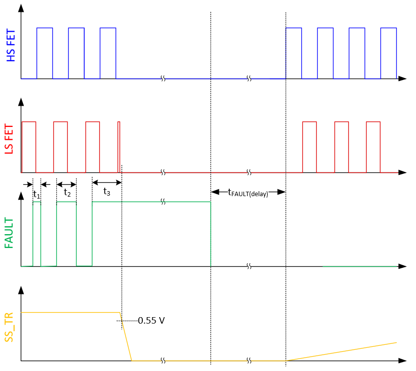
A. The
FAULT waveform is an input signal with a duty cycle that increases until the
device enters fault mode (determined to occur when SS_TR falls to 0.55V).
B. t1, t2 < tFAULT(min)
C. t3 ≥ tFAULT(min)
Figure 7-1 FAULT Minimum Pulse Width and
Delay Duration
A. VREF = VCOMP – VSNS-. This accurate reference voltage
value includes the error amplifier offset, VIO. Use this value to set
the output voltage.
Figure 7-2 Reference Voltage Measurement
A.
Figure 7-3 SYNCx Rise and Fall Time
A.
Figure 7-4 SYNC2 to SYNC1 Rising Edge Phase Shift
A.
Figure 7-5 SYNC1 to SW Delay:
Non-inverted Sync
A.
Figure 7-6 SYNC1 to SW Delay: Inverted
Sync
A.
Figure 7-7 SYNC1 to SW Delay: SYNC1
Output