SNVSA82C April 2015 – October 2017 LM43603-Q1
PRODUCTION DATA.
- 1 Features
- 2 Applications
- 3 Description
- 4 Revision History
- 5 Pin Configuration and Functions
- 6 Specifications
-
7 Detailed Description
- 7.1 Overview
- 7.2 Functional Block Diagram
- 7.3
Feature Description
- 7.3.1 Fixed Frequency Peak Current Mode Controlled Step-Down Regulator
- 7.3.2 Light Load Operation
- 7.3.3 Adjustable Output Voltage
- 7.3.4 Enable (EN)
- 7.3.5 VCC, UVLO, and BIAS
- 7.3.6 Soft-Start and Voltage Tracking (SS/TRK)
- 7.3.7 Switching Frequency (RT) and Synchronization (SYNC)
- 7.3.8 Minimum ON Time, Minimum OFF Time and Frequency Foldback at Dropout Conditions
- 7.3.9 Internal Compensation and CFF
- 7.3.10 Bootstrap Voltage (BOOT)
- 7.3.11 Power Good (PGOOD)
- 7.3.12 Overcurrent and Short-Circuit Protection
- 7.3.13 Thermal Shutdown
- 7.4 Device Functional Modes
-
8 Applications and Implementation
- 8.1 Application Information
- 8.2
Typical Applications
- 8.2.1 Design Requirements
- 8.2.2
Detailed Design Procedure
- 8.2.2.1 Custom Design With WEBENCH® Tools
- 8.2.2.2 Output Voltage Setpoint
- 8.2.2.3 Switching Frequency
- 8.2.2.4 Input Capacitors
- 8.2.2.5 Inductor Selection
- 8.2.2.6 Output Capacitor Selection
- 8.2.2.7 Feed-Forward Capacitor
- 8.2.2.8 Bootstrap Capacitors
- 8.2.2.9 VCC Capacitor
- 8.2.2.10 BIAS Capacitors
- 8.2.2.11 Soft-Start Capacitors
- 8.2.2.12 Undervoltage Lockout Setpoint
- 8.2.2.13 PGOOD
- 8.2.3 Application Performance Curves
- 9 Power Supply Recommendations
- 10Layout
- 11Device and Documentation Support
- 12Mechanical, Packaging, and Orderable Information
10 Layout
The performance of any switching converter depends as much upon the layout of the PCB as the component selection. The following guidelines will help users design a PCB with the best power conversion performance, thermal performance, and minimized generation of unwanted EMI.
10.1 Layout Guidelines
- Place ceramic high frequency bypass CIN as close as possible to the LM43603-Q1 VIN and PGND pins. Grounding for both the input and output capacitors should consist of localized top side planes that connect to the PGND pins and PAD.
- Place bypass capacitors for VCC and BIAS close to the pins and ground the bypass capacitors to device ground.
- Minimize trace length to the FB pin net. Locate both feedback resistors, RFBT and RFBB close to the FB pin. Place CFF directly in parallel with RFBT. If VOUT accuracy at the load is important, make sure VOUT sense is made at the load. Route VOUT sense path away from noisy nodes and preferably through a layer on the other side of a shieldig layer.
- Use ground plane in one of the middle layers as noise shielding and heat dissipation path.
- Have a single point ground connection to the plane. Route the ground connections for the feedback, soft-start, and enable components to the ground plane. This prevents any switched or load currents from flowing in the analog ground traces. If not properly handled, poor grounding can result in degraded load regulation or erratic output voltage ripple behavior.
- Make VIN, VOUT and ground bus connections as wide as possible. This reduces any voltage drops on the input or output paths of the converter and maximizes efficiency.
- Provide adequate device heat sinking. Use an array of heat-sinking vias to connect the exposed pad to the ground plane on the bottom PCB layer. If the PCB has multiple copper layers, these thermal vias can also be connected to inner layer heat-spreading ground planes. Ensure enough copper area is used for heat-sinking to keep the junction temperature below 125°C.
10.1.1 Compact Layout for EMI Reduction
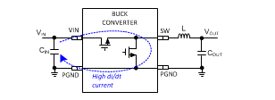
Radiated EMI is generated by the high di/dt components in pulsing currents in switching converters. The larger area covered by the path of a pulsing current, the more EMI is generated. The key to minimize radiated EMI is to identify pulsing current path and minimize the area of the path. In Buck converters,the pulsing current path is from the VIN side of the input capacitors to HS switch, to the LS switch, and then return to the ground of the input capacitors, as shown in Figure 97.
 Figure 97. Buck Converter High Δi/Δt Path
High-frequency ceramic bypass capacitors at the input side provide primary path for the high di/dt components of the pulsing current. Placing ceramic bypass capacitor(s) as close as possible to the VIN and PGND pins is the key to EMI reduction.
The SW pin connecting to the inductor must be as short as possible, and just wide enough to carry the load current without excessive heating. Use short, thick traces or copper pours (shapes) for high current condution path to minimize parasitic resistance. The output capacitors must be place close to the VOUT end of the inductor and closely grounded to PGND pin and exposed PAD.
Place the bypass capacitors on VCC and BIAS pins as close as possible to the pins respectively and closely grounded to PGND and the exposed PAD.
10.1.2 Ground Plane and Thermal Considerations
TI recommends using one of the middle layers as a solid ground plane. Ground plane provides shielding for sensitive circuits and traces. It also provides a quiet reference potential for the control circuitry. The AGND and PGND pins must be connected to the ground plane using vias right next to the bypass capacitors. PGND pins are connected to the source of the internal LS switch. They must be connected directly to the grounds of the input and output capacitors. The PGND net contains noise at switching frequency and may bounce due to load variations. Constrain PGND trace, as well as PVIN and SW traces, to one side of the ground plane. The other side of the ground plane contains much less noise and should be used for sensitive routes.
TI recommends providing adequate device heat sinking by utilizing the PAD of the device as the primary thermal path. Use a recommended 4 by 3 array of 10-mil thermal vias to connect the PAD to the system ground plane heat sink. The vias must be evenly distributed under the PAD. Use as much copper as possible, for system ground plane, on the top and bottom layers for the best heat dissipation. Use a four-layer board with the copper thickness for the four layers, starting from the top of, 2 oz / 1 oz / 1 oz / 2 oz. Four layer boards with enough copper thickness provides low current conduction impedance, proper shielding and lower thermal resistance.
The thermal characteristics of the LM43603-Q1 are specified using the parameter RθJA, which characterize the junction temperature of silicon to the abient temperature in a specific system. Although the value of RθJA is dependant on manhy variables, it still can be used to approximate the operating junction temperature of the device. To obtain an estimate of the device junction temperature, one may use Equation 27:
where
- TJ = Junction temperature in °C
- PD = VIN x IIN × (1 - Efficiency) – 1.1 x IOUT × DCR
- RθJA = junction-to-ambient thermal resistance of the device in °C/W
- DCR = inductor DC parasitic resistance in Ω
- TA = ambient temperature in °C
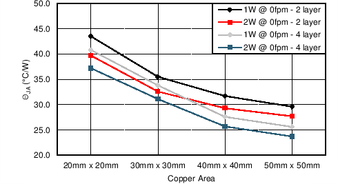
The maximum operating junction temperature of the LM43603-Q1 is 125°C. RθJA is highly related to PCB size and layout, as well as enviromental factors such as heat sinking and air flow. Figure 98 shows measured results of RθJA with different copper area on a 2-layer board and 4-layer board.
 Figure 98. RθJAvs Copper Area
 2 oz Copper on Outer Layers and 1 oz Copper on Inner Layers
10.1.3 Feedback Resistors
To reduce noise sensitivity of the output voltage feedback path, it is important to place the resistor divider and CFF close to the FB pin, rather than close to the load. The FB pin is the input to the error amplifier, so it is a high impedance node and very sensitive to noise. Placing the resistor divider and CFF closer to the FB pin reduces the trace length of FB signal and reduces noise coupling. The output node is a low impedance node, so the trace from VOUT to the resistor divider can be long if short path is not available.
If voltage accuracy at the load is important, make sure voltage sense is made at the load. Doing so corrects for voltage drops along the traces and provide the best output accuracy. The voltage sense trace from the load to the feedback resistor divider must be routed away from the SW node path and the inductor to avoid contaminating the feedback signal with switch noise, while also minimizing the trace length. This is most important when high value resistors are used to set the output voltage. TI recommends routing the voltage sense trace and place the resistor divider on a different layer than the inductor and SW node path, such that there is a ground plane in between the feedback trace and inductor/SW node polygon. This provides further shielding for the voltage feedback path from EMI noises.
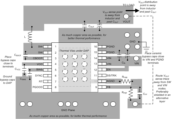
10.2 Layout Example
 Figure 99. LM43603-Q1 Board Layout Recommendations