SNVSAF7B August 2016 – February 2017 LM27762
PRODUCTION DATA.
- 1 Features
- 2 Applications
- 3 Description
- 4 Revision History
- 5 Pin Configuration and Functions
- 6 Specifications
- 7 Detailed Description
-
8 Application and Implementation
- 8.1 Application Information
- 8.2
Typical Application
- 8.2.1 Design Requirements
- 8.2.2 Detailed Design Procedure
- 8.2.3 Application Curves
- 9 Power Supply Recommendations
- 10Layout
- 11Device and Documentation Support
- 12Mechanical, Packaging, and Orderable Information
5 Pin Configuration and Functions
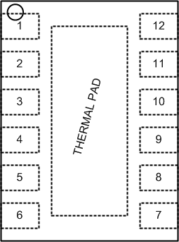
DSS Package
12-Pin WSON With Thermal Pad
Top View

Pin Functions
| PIN | TYPE | DESCRIPTION | |
|---|---|---|---|
| NAME | NUMBER | ||
| C1+ | 10 | Power | Positive terminal for C1 |
| C1– | 9 | Power | Negative terminal for C1 |
| CP | 5 | Power | Negative unregulated output voltage |
| EN+ | 12 | Input | Enable input for the positive LDO, Active high |
| EN– | 8 | Input | Enable input for the charge pump and negative LDO, Active high |
| FB+ | 2 | Power | Feedback input. Connect FB+ to an external resistor divider between OUT+ and GND. DO NOT leave unconnected. |
| FB– | 7 | Power | Feedback input. Connect FB– to an external resistor divider between OUT– and GND. DO NOT leave unconnected. |
| GND | 4 | Ground | Ground |
| OUT+ | 11 | Power | Regulated positive output voltage |
| OUT– | 6 | Power | Regulated negative output voltage |
| PGOOD | 1 | Output | Power Good flag; open drain; Logic 0 = power good, Logic 1 = power not good. Connect to ground if not used. |
| VIN | 3 | Power | Positive power supply input |
| Thermal Pad | — | Ground | Ground. DO NOT leave unconnected. |