SNVSAI4B November 2017 – November 2020 LM5145
PRODUCTION DATA
- 1 Features
- 2 Applications
- 3 Description
- 4 Revision History
- 5 Description (continued)
- 6 Pin Configuration and Functions
- 7 Specifications
-
8 Detailed Description
- 8.1 Overview
- 8.2 Functional Block Diagram
- 8.3
Feature Description
- 8.3.1 Input Range (VIN)
- 8.3.2 Output Voltage Setpoint and Accuracy (FB)
- 8.3.3 High-Voltage Bias Supply Regulator (VCC)
- 8.3.4 Precision Enable (EN/UVLO)
- 8.3.5 Power Good Monitor (PGOOD)
- 8.3.6 Switching Frequency (RT, SYNCIN)
- 8.3.7 Configurable Soft Start (SS/TRK)
- 8.3.8 Voltage-Mode Control (COMP)
- 8.3.9 Gate Drivers (LO, HO)
- 8.3.10 Current Sensing and Overcurrent Protection (ILIM)
- 8.3.11 OCP Duty Cycle Limiter
- 8.4 Device Functional Modes
-
9 Application and Implementation
- 9.1 Application Information
- 9.2
Typical Applications
- 9.2.1 Design 1 – 20-A High-Efficiency Synchronous Buck Regulator for Telecom Power Applications
- 9.2.2 Design 2 – High Density, 12-V, 10-A Rail With LDO Low-Noise Auxiliary Output for RF Power Applications
- 9.2.3 Design 3 – 150-W, Regulated 24-V Rail for Commercial Drone Applications With Output Voltage Tracking Feature
- 9.2.4 Design 4 – Powering a Multicore DSP From a 24-V or 48-V Rail
- 10Power Supply Recommendations
- 11Layout
- 12Device and Documentation Support
- 13Mechanical, Packaging, and Orderable Information
9.2.1 Design 1 – 20-A High-Efficiency Synchronous Buck Regulator for Telecom Power Applications
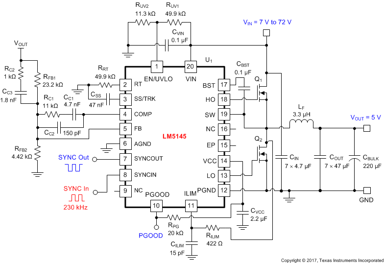
Figure 9-5 shows the schematic diagram of a 5-V, 20-A buck regulator with a switching frequency of 230 kHz. In this example, the target half-load and full-load efficiencies are 93.5% and 92.5%, respectively, based on a nominal input voltage of 48 V that ranges from 7 V to 72 V. The switching frequency is set by means of a synchronization input signal at 230 kHz, and the free-running switching frequency (in the event that the synchronization signal is removed) is set at 200 kHz by resistor RRT. In terms of control loop performance, the target loop crossover frequency is 35 kHz with a phase margin greater than 50°. The output voltage soft-start time is 4 ms.
 Figure 9-5 Application Circuit 1 With LM5145 48-V to 5-V, 20-A Buck Regulator at 230 kHz
This and subsequent design examples are provided herein to showcase the LM5145 controller in several different applications. Depending on the source impedance of the input supply bus, an electrolytic capacitor may be required at the input to ensure stability, particularly at low input voltage and high output current operating conditions. See Section 10 for more detail.