SNVSAO6C September   2017  – March 2018 LMZM33603

PRODUCTION DATA.  

  1. Features
  2. Applications
    1.     Simplified Schematic
  3. Description
    1.     Safe Operating Area
  4. Revision History
  5. Pin Configuration and Functions
    1.     Pin Functions
  6. Specifications
    1. 6.1 Absolute Maximum Ratings
    2. 6.2 ESD Ratings
    3. 6.3 Recommended Operating Conditions
    4. 6.4 Thermal Information
    5. 6.5 Electrical Characteristics
    6. 6.6 Switching Characteristics
    7. 6.7 Typical Characteristics (VIN = 5 V)
    8. 6.8 Typical Characteristics (VIN = 12 V)
    9. 6.9 Typical Characteristics (VIN = 24 V)
  7. Detailed Description
    1. 7.1 Overview
    2. 7.2 Functional Block Diagram
    3. 7.3 Feature Description
      1. 7.3.1  Adjusting the Output Voltage
      2. 7.3.2  Feed-Forward Capacitor, CFF
      3. 7.3.3  Output Current vs Output Voltage
      4. 7.3.4  Voltage Dropout
      5. 7.3.5  Switching Frequency (RT)
      6. 7.3.6  Synchronization (SYNC)
      7. 7.3.7  Input Capacitors
      8. 7.3.8  Output Capacitors
      9. 7.3.9  Output On/Off Enable (EN)
      10. 7.3.10 Programmable Undervoltage Lockout (UVLO)
      11. 7.3.11 Power Good (PGOOD)
      12. 7.3.12 Overcurrent Protection (OCP)
      13. 7.3.13 Thermal Shutdown
    4. 7.4 Device Functional Modes
      1. 7.4.1 Active Mode
      2. 7.4.2 Shutdown Mode
  8. Application and Implementation
    1. 8.1 Application Information
    2. 8.2 Typical Application
      1. 8.2.1 Design Requirements
      2. 8.2.2 Detailed Design Procedure
        1. 8.2.2.1 Custom Design With WEBENCH® Tools
        2. 8.2.2.2 Output Voltage Setpoint
        3. 8.2.2.3 Feed-Forward Capacitor (CFF)
        4. 8.2.2.4 Setting the Switching Frequency
        5. 8.2.2.5 Input Capacitors
        6. 8.2.2.6 Output Capacitor Selection
        7. 8.2.2.7 Application Curves
  9. Power Supply Recommendations
  10. 10Layout
    1. 10.1 Layout Guidelines
    2. 10.2 Layout Examples
    3. 10.3 Theta JA vs PCB Area
    4. 10.4 EMI
      1. 10.4.1 EMI Plots
    5. 10.5 Package Specifications
  11. 11Device and Documentation Support
    1. 11.1 Device Support
      1. 11.1.1 Third-Party Products Disclaimer
      2. 11.1.2 Custom Design With WEBENCH® Tools
    2. 11.2 Related Documentation
    3. 11.3 Receiving Notification of Documentation Updates
    4. 11.4 Community Resources
    5. 11.5 Trademarks
    6. 11.6 Electrostatic Discharge Caution
    7. 11.7 Glossary
  12. 12Mechanical, Packaging, and Orderable Information
    1. 12.1 Tape and Reel Information

EMI Plots

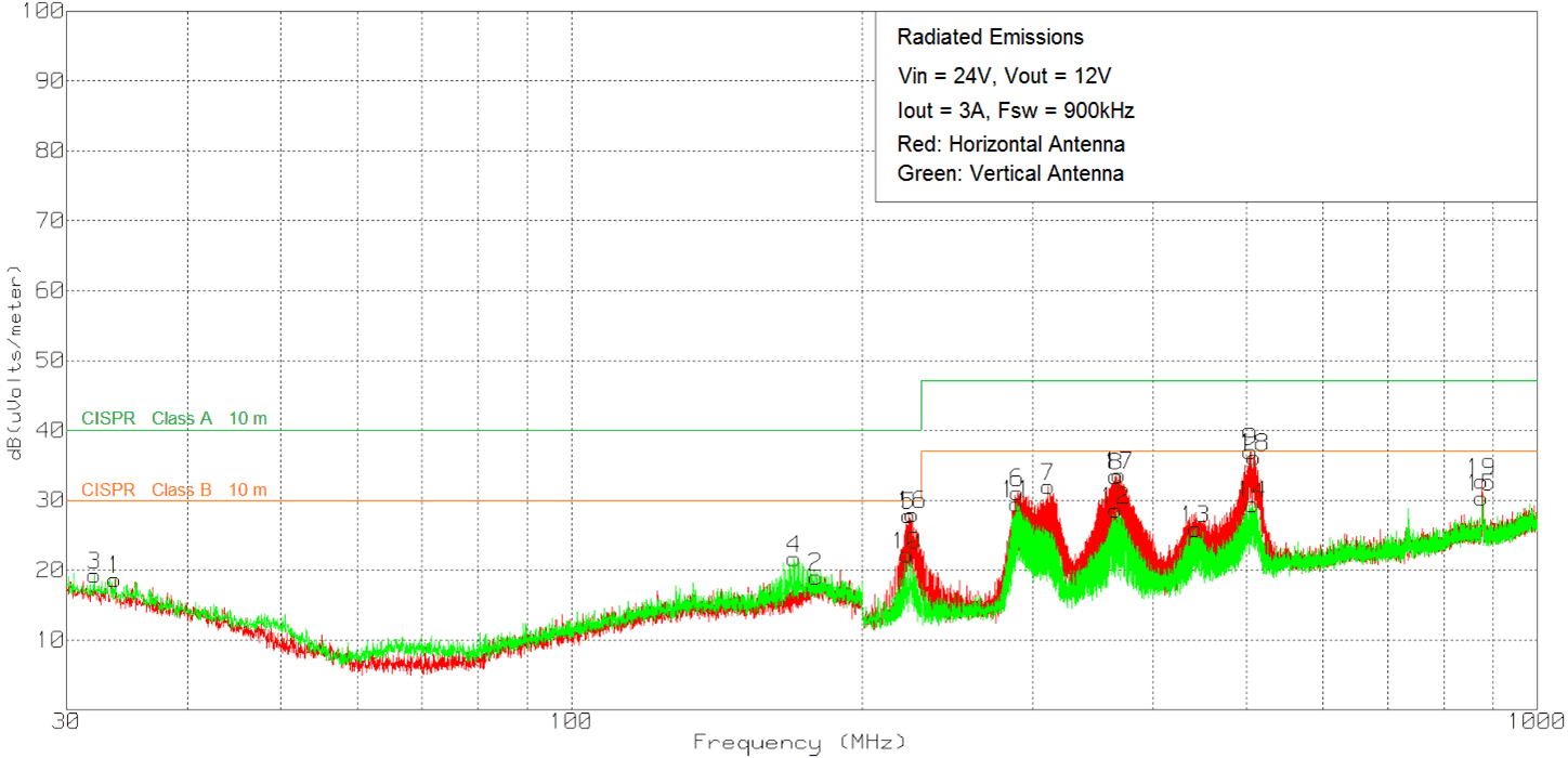
EMI plots were measured using the standard LMZM33603EVM with no input filter.
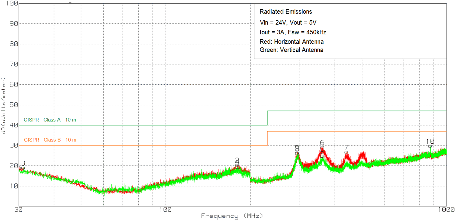
LMZM33603 EMI24_5.gif
Figure 43. Radiated Emissions 24-V Input, 5-V Output, 3-A Load (EN55011 Class B)
LMZM33603 EMI24_12.gifFigure 44. Radiated Emissions 24-V Input, 12-V Output, 3-A Load (EN55011 Class B)
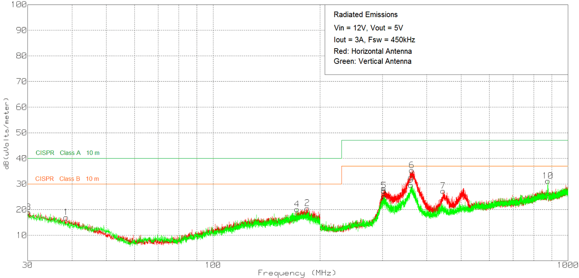
LMZM33603 EMI12_5.gif
Figure 45. Radiated Emissions 12-V Input, 5-V Output, 3-A Load (EN55011 Class B)