SNVSAP9A March 2017 – February 2018 LM25141-Q1
PRODUCTION DATA.
- 1 Features
- 2 Applications
- 3 Description
- 4 Revision History
- 5 Pin Configuration and Functions
- 6 Specifications
-
7 Detailed Description
- 7.1 Overview
- 7.2 Functional Block Diagram
- 7.3
Feature Description
- 7.3.1 High Voltage Start-Up Regulator
- 7.3.2 VCC Regulator
- 7.3.3 Oscillator
- 7.3.4 Synchronization
- 7.3.5 Frequency Dithering (Spread Spectrum)
- 7.3.6 Enable
- 7.3.7 Power Good
- 7.3.8 Output Voltage
- 7.3.9 Current Sense
- 7.3.10 DCR Current Sensing
- 7.3.11 Error Amplifier and PWM Comparator
- 7.3.12 Slope Compensation
- 7.3.13 Hiccup Mode Current Limiting
- 7.3.14 Standby Mode
- 7.3.15 Soft Start
- 7.3.16 Diode Emulation
- 7.3.17 High- and Low-Side Drivers
-
8 Application and Implementation
- 8.1 Application Information
- 8.2 Typical Application
- 9 Power Supply Recommendations
- 10Layout
- 11Device and Documentation Support
- 12Mechanical, Packaging, and Orderable Information
7.3.8 Output Voltage
The LM25141-Q1 output can be configured for one of the two fixed output voltages with no external feedback resistors, or the output can be adjusted to the desired voltage using an external resistor divider. VOUT can be configured as a 3.3-V output by connecting the FB pin to VDDA, or a 5-V output by connecting the FB pin to ground with a maximum resistance of 500 Ω. The FB connections (either VDDA or GND) are detected during power up.
The configuration setting is latched and cannot be changed until the LM25141-Q1 is powered down with VCC falling below VCC(UVLO) (3.4 V typical) and then powered up again.
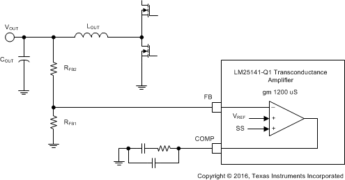
Alternatively the output voltage can be set using an external resistive dividers from the output to the FB pin. The output voltage adjustment range is between 1.5 V and 15 V. The regulation threshold at the FB pin is 1.2 V (VREF). To calculate RFB1 and RFB2 use Equation 4. Refer to Figure 23:

The recommend starting point is to select RFB1 between 10 kΩ to 20 kΩ.
The Thevenin equivalent impedance of the resistive divider connected to the FB pin must be greater than 5 kΩ for the LM25141-Q1 to detect the divider and set the controller to the adjustable output mode. Refer to Equation 5.

If a low IQ mode is required, take care when selecting the external resistors. The extra current drawn from the external divider is added to the LM25141-Q1 ISTANDBY current (35 μA typical). The divider current reflected to VIN is divided down by the ratio of VOUT/VIN. For example, if VIN is 12V and VOUT is set to 5.5 V with RFB1 10 kΩ, and RFB2 = 35.7 kΩ, the input current at VIN required to supply the current in the feedback resistors is:

where
- VIN = 12 V
The total input current in this condition is:

 Figure 23. Voltage Feedback