-
UCC27282 3-A 120-V Half-Bridge Driver with Cross Conduction Protection and Low Switching Losses
- 1 Features
- 2 Applications
- 3 Description
- 4 Revision History
- 5 Pin Configuration and Functions
- 6 Specifications
- 7 Detailed Description
- 8 Application and Implementation
- 9 Power Supply Recommendations
- 10Layout
- 11Device and Documentation Support
- 12Mechanical, Packaging, and Orderable Information
- IMPORTANT NOTICE
UCC27282 3-A 120-V Half-Bridge Driver with Cross Conduction Protection and Low Switching Losses
1 Features
- Drives two N-channel MOSFETs in high-side low-side configuration
- 5-V typical under voltage lockout
- Input interlock
- Enable/disable functionality in DRC package
- 16-ns typical propagation delay
- 12-ns rise, 10-ns fall time with 1.8-nF load
- 1-ns typical delay matching
- Absolute Maximum Negative Voltage Handling on Inputs (–5 V)
- Absolute Maximum Negative Voltage Handling on HS (–14 V)
- ±3-A peak output current
- Absolute maximum boot voltage 120 V
- Low current (7-µA) consumption when disabled
- Integrated bootstrap diode
- Specified from –40°C to 140°C junction temperature
2 Applications
- Telecom and merchant power supplies
- Motor drives and power tools
- Auxiliary inverters
- Half-bridge and full-bridge converters
- Active-clamp forward converters
- High voltage synchronous-buck converters
- Class-D audio amplifiers
 Simplified Application Diagram
3 Description
The UCC27282 is a robust N-channel MOSFET driver with a maximum switch node (HS) voltage rating of 100 V. It allows for two N-channel MOSFETs to be controlled in half-bridge or synchronous buck configuration based topologies. Its 3-A peak source and sink current along with low pull-up and pull-down resistance allows the UCC27282 to drive large power MOSFETs with minimum switching losses during the transition of the MOSFET Miller plateau. Since the inputs are independent of the supply voltage, UCC27282 can be used in conjunction with both analog and digital controllers.
The input pins as well as the HS pin are able to tolerate significant negative voltage, which improves system robustness. Input interlock further improves robustness and system reliability in high noise applications. The enable and disable functionality provides additional system flexibility by reducing power consumption by the driver and responds to fault events within the system. 5-V UVLO allows systems to operate at lower bias voltages, which is necessary in many high frequency applications and improves system efficiency in certain operating modes. Small propagation delay and delay matching specifications minimize the dead-time requirement which further improves efficiency.
Under voltage lockout (UVLO) is provided for both the high-side and low-side driver stages forcing the outputs low if the VDD voltage is below the specified threshold. An integrated bootstrap diode eliminates the need for an external discrete diode in many applications, which saves board space and reduces system cost. UCC27282 is offered in a small package enabling high density designs.
| PART NUMBER | PACKAGE (SIZE) |
|---|---|
| UCC27282 | SON10 (3 mm x 3 mm) |
| SOIC8 (6 mm x 5mm)) | |
| SON8 (4 mm x 4 mm) | |
| SON10 (4 mm x 4 mm) |
4 Revision History
Changes from Revision A (January 2020) to Revision B (May 2022)
- Added SON 8-Pin DRM and SON 10-pin DPR packages to the Device Information table.Go
- Added SON 8-Pin DRM and SON 10-pin DPR package images and updated the Pin Functions table.Go
- Added SON 8-pin DRM and SON 10-pin DPR packages to Thermal Information.Go
- Updated typcal peak pullup/pulldown current from +2.5A/-3.5A to ±3A in Electrical CharacteristicsGo
- Updated IHBS typical leakage to 5.0μA and test voltage from 110V to 100V in Electrical CharacteristicsGo
5 Pin Configuration and Functions
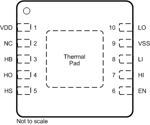
 Figure 5-1 DRC Package10-Pin VSON With Exposed Thermal PadTop View
 Figure 5-3 DRM Package8-Pin SONTop View
 Figure 5-2 D Package8-Pin SOICTop View
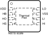
 Figure 5-4 DPR Package10-Pin SONTop View
| PIN | I/O(1) | DESCRIPTION | |||||
|---|---|---|---|---|---|---|---|
| Name | D | DRC | DRM | DPR | |||
| EN | n/a | 6 | n/a | n/a | I | Enable input. When this pin is pulled high, it will enable the driver. If left floating or pulled low, it will disable the driver. 1 nF filter capacitor is recommended for high-noise systems. | |
| HB | 2 | 3 | 2 | 2 | P | High-side bootstrap supply. The bootstrap diode is on-chip but the external bootstrap capacitor is required. Connect positive side of the bootstrap capacitor to this pin. Typical recommended value of HB bypass capacitor is 0.1 μF, This value primarily depends on the gate charge of the high-side MOSFET. When using external boot diode, connect cathode of the diode to this pin. | |
| HI | 5 | 7 | 5 | 7 | I | High-side input. | |
| HO | 3 | 4 | 3 | 3 | O | High-side output. Connect to the gate of the high-side power MOSFET or one end of external gate resistor, when used. | |
| HS | 4 | 5 | 4 | 4 | P | High-side source connection. Connect to source of high-side power MOSFET. Connect negative side of bootstrap capacitor to this pin. | |
| LI | 6 | 8 | 6 | 8 | I | Low-side input | |
| LO | 8 | 10 | 8 | 10 | O | Low-side output. Connect to the gate of the low-side power MOSFET or one end of external gate resistor, when used. | |
| NC | n/a | 2 | n/a | 5,6 | — | Not connected internally. | |
| VDD | 1 | 1 | 1 | 1 | P | Positive supply to the low-side gate driver. Decouple this pin to VSS. Typical decoupling capacitor value is 1 μF. When using an external boot diode, connect the anode to this pin. | |
| VSS | 7 | 9 | 7 | 9 | G | Negative supply terminal for the device which is generally the system ground. | |
| Thermal pad | n/a | - | - | - | — | Connect to a large thermal mass trace (generally IC ground plane) to improve thermal performance. This can only be electrically connected to VSS. | |