SNVSAQ5B November 2018 – May 2022 UCC27282
PRODUCTION DATA
- 1 Features
- 2 Applications
- 3 Description
- 4 Revision History
- 5 Pin Configuration and Functions
- 6 Specifications
- 7 Detailed Description
- 8 Application and Implementation
- 9 Power Supply Recommendations
- 10Layout
- 11Device and Documentation Support
- 12Mechanical, Packaging, and Orderable Information
5 Pin Configuration and Functions
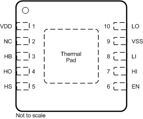
 Figure 5-1 DRC Package10-Pin VSON With Exposed Thermal PadTop View
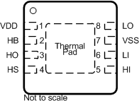
 Figure 5-3 DRM Package8-Pin SONTop View
 Figure 5-2 D Package8-Pin SOICTop View
 Figure 5-4 DPR Package10-Pin SONTop View
Table 5-1 Pin Functions
| PIN | I/O(1) | DESCRIPTION | |||||
|---|---|---|---|---|---|---|---|
| Name | D | DRC | DRM | DPR | |||
| EN | n/a | 6 | n/a | n/a | I | Enable input. When this pin is pulled high, it will enable the driver. If left floating or pulled low, it will disable the driver. 1 nF filter capacitor is recommended for high-noise systems. | |
| HB | 2 | 3 | 2 | 2 | P | High-side bootstrap supply. The bootstrap diode is on-chip but the external bootstrap capacitor is required. Connect positive side of the bootstrap capacitor to this pin. Typical recommended value of HB bypass capacitor is 0.1 μF, This value primarily depends on the gate charge of the high-side MOSFET. When using external boot diode, connect cathode of the diode to this pin. | |
| HI | 5 | 7 | 5 | 7 | I | High-side input. | |
| HO | 3 | 4 | 3 | 3 | O | High-side output. Connect to the gate of the high-side power MOSFET or one end of external gate resistor, when used. | |
| HS | 4 | 5 | 4 | 4 | P | High-side source connection. Connect to source of high-side power MOSFET. Connect negative side of bootstrap capacitor to this pin. | |
| LI | 6 | 8 | 6 | 8 | I | Low-side input | |
| LO | 8 | 10 | 8 | 10 | O | Low-side output. Connect to the gate of the low-side power MOSFET or one end of external gate resistor, when used. | |
| NC | n/a | 2 | n/a | 5,6 | — | Not connected internally. | |
| VDD | 1 | 1 | 1 | 1 | P | Positive supply to the low-side gate driver. Decouple this pin to VSS. Typical decoupling capacitor value is 1 μF. When using an external boot diode, connect the anode to this pin. | |
| VSS | 7 | 9 | 7 | 9 | G | Negative supply terminal for the device which is generally the system ground. | |
| Thermal pad | n/a | - | - | - | — | Connect to a large thermal mass trace (generally IC ground plane) to improve thermal performance. This can only be electrically connected to VSS. | |
(1) P = Power, G = Ground, I = Input, O = Output, I/O =
Input/Output