SNVSB11B June 2018 – May 2019 LMZM33606
PRODUCTION DATA.
- 1 Features
- 2 Applications
- 3 Description
- 4 Revision History
- 5 Pin Configuration and Functions
- 6 Specifications
-
7 Detailed Description
- 7.1 Overview
- 7.2 Functional Block Diagram
- 7.3
Feature Description
- 7.3.1 Adjusting the Output Voltage
- 7.3.2 Input Capacitor Selection
- 7.3.3 Output Capacitor Selection
- 7.3.4 Transient Response
- 7.3.5 Feed-Forward Capacitor
- 7.3.6 Switching Frequency (RT)
- 7.3.7 Synchronization (SYNC/MODE)
- 7.3.8 Output Enable (EN)
- 7.3.9 Programmable System UVLO (EN)
- 7.3.10 Internal LDO and BIAS_SEL
- 7.3.11 Power Good (PGOOD) and Power Good Pull-Up (PGOOD_PU)
- 7.3.12 Mode Select (Auto or FPWM)
- 7.3.13 Soft Start and Voltage Tracking
- 7.3.14 Voltage Dropout
- 7.3.15 Overcurrent Protection (OCP)
- 7.3.16 Thermal Shutdown
- 7.4 Device Functional Modes
- 8 Application and Implementation
- 9 Power Supply Recommendations
- 10Layout
- 11Device and Documentation Support
- 12Mechanical, Packaging, and Orderable Information
3 Description
The LMZM33606 power module is an easy-to-use integrated power solution that combines a 6-A DC/DC converter with power MOSFETs, a shielded inductor, and passives in a low-profile package. This power solution requires as few as four external components and eliminates the loop compensation and inductor part selection from the design process.
The 16 mm × 10 mm × 4 mm, 41-pin, QFN package is easy to solder onto a printed circuit board and allows a compact, low-profile point-of-load design. The LMZM33606 feature set includes power good, adjustable soft start, tracking, synchronization, programmable UVLO, prebias start-up, selectable auto or FPWM modes, as well as over-current and over-temperature protection. The LMZM33606 can be configured as negative output voltage for inverting applications.
Device Information
| DEVICE NUMBER | PACKAGE | BODY SIZE (NOM) |
|---|---|---|
| LMZM33606 | QFN (41) | 16.00 mm × 10.00 mm |
space
Minimum Solution Size

space
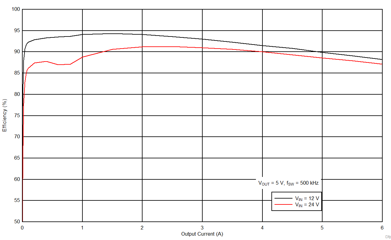
Typical Efficiency (Auto Mode)
