SNVSB48C April   2018  – October 2019 LMR36006

PRODUCTION DATA.  

  1. Features
  2. Applications
  3. Description
    1.     Device Images
      1.      Simplified Schematic
  4. Revision History
  5. Device Comparison Table
  6. Pin Configuration and Functions
    1.     Pin Functions
  7. Specifications
    1. 7.1 Absolute Maximum Ratings
    2. 7.2 ESD Ratings
    3. 7.3 Recommended Operating Conditions
    4. 7.4 Thermal Information
    5. 7.5 Electrical Characteristics
    6. 7.6 Timing Requirements
    7. 7.7 System Characteristics
    8. 7.8 Typical Characteristics
  8. Detailed Description
    1. 8.1 Overview
    2. 8.2 Functional Block Diagram
    3. 8.3 Feature Description
      1. 8.3.1 Power-Good Flag Output
      2. 8.3.2 Enable and Start-up
      3. 8.3.3 Current Limit and Short Circuit
      4. 8.3.4 Undervoltage Lockout and Thermal Shutdown
    4. 8.4 Device Functional Modes
      1. 8.4.1 Auto Mode
      2. 8.4.2 Dropout
      3. 8.4.3 Minimum Switch On-Time
  9. Application and Implementation
    1. 9.1 Application Information
    2. 9.2 Typical Application
      1. 9.2.1 Design 1: Low Power 24-V, 600-mA PFM Converter
        1. 9.2.1.1 Design Requirements
        2. 9.2.1.2 Detailed Design Procedure
          1. 9.2.1.2.1  Custom Design With WEBENCH Tools
          2. 9.2.1.2.2  Choosing the Switching Frequency
          3. 9.2.1.2.3  Setting the Output Voltage
          4. 9.2.1.2.4  Inductor Selection
          5. 9.2.1.2.5  Output Capacitor Selection
          6. 9.2.1.2.6  Input Capacitor Selection
          7. 9.2.1.2.7  CBOOT
          8. 9.2.1.2.8  VCC
          9. 9.2.1.2.9  CFF Selection
            1. 9.2.1.2.9.1 External UVLO
          10. 9.2.1.2.10 Maximum Ambient Temperature
      2. 9.2.2 Application Curves
      3. 9.2.3 Design 2: High Density 24-V, 600-mA PFM Converter
        1. 9.2.3.1 Design Requirements
        2. 9.2.3.2 Application Curves
    3. 9.3 What to Do and What Not to Do
  10. 10Power Supply Recommendations
  11. 11Layout
    1. 11.1 Layout Guidelines
      1. 11.1.1 Ground and Thermal Considerations
    2. 11.2 Layout Example
  12. 12Device and Documentation Support
    1. 12.1 Device Support
      1. 12.1.1 Development Support
        1. 12.1.1.1 Custom Design With WEBENCH® Tools
    2. 12.2 Documentation Support
      1. 12.2.1 Related Documentation
    3. 12.3 Receiving Notification of Documentation Updates
    4. 12.4 Support Resources
    5. 12.5 Trademarks
    6. 12.6 Electrostatic Discharge Caution
    7. 12.7 Glossary
  13. 13Mechanical, Packaging, and Orderable Information

Typical Characteristics

Unless otherwise specified the following conditions apply: TA = 25°C. VIN = 24 V.
LMR36006 LMR36006B-Non-switching-Iq.gif
VFB = 1 V
Figure 1. Non-Switching Input Supply Current
LMR36006 hs-cl-lmr36006.gif
VIN = 24 V
Figure 3. High Side Current Limit
LMR36006 vref.gif
Figure 5. Reference Voltage Drift
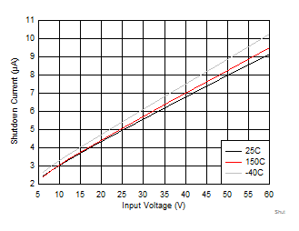
LMR36006 ShutdownCurrent_temp.gif
EN = 0 V
Figure 2. Shutdown Supply Current
LMR36006 ls-cl-lmr36006.gif
VIN = 24 V
Figure 4. Low Side Current Limit
LMR36006 LMR36006B_I-Min-Pk.gif
IOUT = 0 A VOUT = 3.3 V
ƒSW = 1000 kHz
Figure 6. IPEAK-MIN