SNVSB55H
February 2019 – June 2024
LM63615-Q1
,
LM63625-Q1
PRODUCTION DATA
1
1
Features
2
Applications
3
Description
4
Device Comparison Table
5
Pin Configuration and Functions
6
Specifications
Absolute Maximum Ratings
6.1
ESD Ratings
6.2
Recommended Operating Conditions
6.3
Thermal Information
6.4
Electrical Characteristics
6.5
Timing Characteristics
6.6
Switching Characteristics
6.7
System Characteristics
6.8
Typical Characteristics
7
Detailed Description
7.1
Overview
7.2
Functional Block Diagram
7.3
Feature Description
7.3.1
Sync/Mode Selection
7.3.2
Output Voltage Selection
7.3.3
Switching Frequency Selection
7.3.3.1
Spread Spectrum Option
7.3.4
Enable and Start-Up
7.3.5
RESET Flag Output
7.3.6
Undervoltage Lockout and Thermal Shutdown and Output Discharge
7.4
Device Functional Modes
7.4.1
Overview
7.4.2
Light Load Operation
7.4.2.1
Sync/FPWM Operation
7.4.3
Dropout Operation
7.4.4
Minimum On-time Operation
7.4.5
Current Limit and Short-Circuit Operation
8
Application and Implementation
8.1
Application Information
8.2
Typical Application
8.2.1
Design Requirements
8.2.2
Detailed Design Procedure
8.2.2.1
Choosing the Switching Frequency
8.2.2.2
Setting the Output Voltage
8.2.2.2.1
CFF Selection
8.2.2.3
Inductor Selection
8.2.2.4
Output Capacitor Selection
8.2.2.5
Input Capacitor Selection
8.2.2.6
CBOOT
8.2.2.7
VCC
8.2.2.8
External UVLO
8.2.2.9
Maximum Ambient Temperature
8.2.3
Full Feature Design Example
8.2.4
Application Curves
8.2.5
EMI Performance Curves
8.3
Best Design Practices
8.4
Power Supply Recommendations
8.5
Layout
8.5.1
Layout Guidelines
8.5.1.1
Ground and Thermal Considerations
8.5.2
Layout Example
9
Device and Documentation Support
9.1
Device Support
9.1.1
Device Nomenclature
9.2
Documentation Support
9.2.1
Related Documentation
9.3
Receiving Notification of Documentation Updates
9.4
Support Resources
9.5
Trademarks
9.6
Electrostatic Discharge Caution
9.7
Glossary
10
Revision History
11
Mechanical, Packaging, and Orderable Information
8.5.2
Layout Example
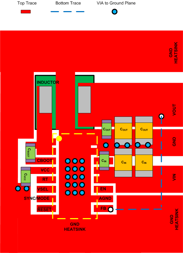
Figure 8-49
Example Layout for HTSSOP Package
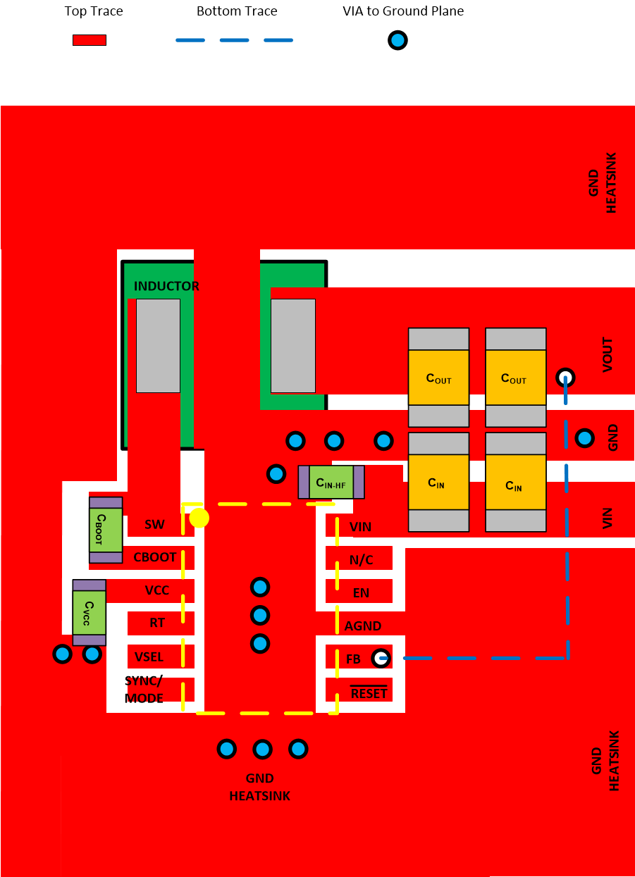
Figure 8-50
Example Layout for WSON Package
Figure 8-51
Example Layout for WSON Package 2nd pinout