SNVSB70F May 2019 – June 2021 LM61460-Q1
PRODUCTION DATA
- 1 Features
- 2 Applications
- 3 Description
- 4 Revision History
- 5 Description (continued)
- 6 Device Comparison Table
- 7 Pin Configuration and Functions
- 8 Specifications
-
9 Detailed Description
- 9.1 Overview
- 9.2 Functional Block Diagram
- 9.3
Feature Description
- 9.3.1 EN/SYNC Uses for Enable and VIN UVLO
- 9.3.2 EN/SYNC Pin Uses for Synchronization
- 9.3.3 Clock Locking
- 9.3.4 Adjustable Switching Frequency
- 9.3.5 PGOOD Output Operation
- 9.3.6 Internal LDO, VCC UVLO, and BIAS Input
- 9.3.7 Bootstrap Voltage and VCBOOT-UVLO (CBOOT Pin)
- 9.3.8 Adjustable SW Node Slew Rate
- 9.3.9 Spread Spectrum
- 9.3.10 Soft Start and Recovery From Dropout
- 9.3.11 Output Voltage Setting
- 9.3.12 Overcurrent and Short Circuit Protection
- 9.3.13 Thermal Shutdown
- 9.3.14 Input Supply Current
- 9.4 Device Functional Modes
-
10Application and Implementation
- 10.1 Application Information
- 10.2
Typical Application
- 10.2.1 Design Requirements
- 10.2.2
Detailed Design Procedure
- 10.2.2.1 Choosing the Switching Frequency
- 10.2.2.2 Setting the Output Voltage
- 10.2.2.3 Inductor Selection
- 10.2.2.4 Output Capacitor Selection
- 10.2.2.5 Input Capacitor Selection
- 10.2.2.6 BOOT Capacitor
- 10.2.2.7 BOOT Resistor
- 10.2.2.8 VCC
- 10.2.2.9 BIAS
- 10.2.2.10 CFF and RFF Selection
- 10.2.2.11 External UVLO
- 10.2.3 Application Curves
- 11Power Supply Recommendations
- 12Layout
- 13Device and Documentation Support
- 14Mechanical, Packaging, and Orderable Information
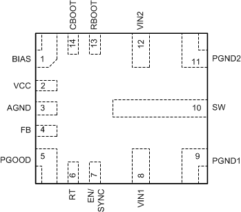
7 Pin Configuration and Functions
 Figure 7-1 14-Pin VQFN-HR RJR Package Top
View
Figure 7-1 14-Pin VQFN-HR RJR Package Top
ViewTable 7-1 Pin Functions
| PIN | I/O | DESCRIPTION | |
|---|---|---|---|
| NAME | NO. | ||
| BIAS | 1 | P | Input to internal LDO. Connect to output voltage point to improve efficiency. Connect an optional high quality 0.1-µF to 1-µF capacitor from this pin to ground for improved noise immunity. If output voltage is above 12 V, connect this pin to ground. |
| VCC | 2 | O | Internal LDO output. Used as supply to internal control circuits. Do not connect to any external loads. Connect a high-quality 1-µF capacitor from this pin to AGND. |
| AGND | 3 | G | Analog ground for internal circuitry. Feedback and VCC are measured with respect to this pin. Must connect AGND to both PGND1 and PGND2 on PCB. |
| FB | 4 | I | Output voltage feedback input to the internal control loop. Connect to feedback divider tap point for adjustable output voltage. Do not float or connect to ground. |
| PGOOD | 5 | O | Open-drain power-good status output. Pull this pin up to a suitable voltage supply through a current limiting resistor. High = power OK, low = fault. PGOOD output goes low when EN = low, VIN > 1 V. |
| RT | 6 | I/O | Connect this pin to ground through a resistor with value between 5.76 kΩ and 66.5 kΩ to set switching frequency between 200 kHz and 2200 kHz. Do not float or connect to ground. |
| EN/SYNC | 7 | I | Precision enable input. High = on, Low = off. Can be connected to VIN. Precision enable allows the pin to be used as an adjustable UVLO. See Section 10. Do not float. EN/SYNC also functions as a synchronization input pin. Triggers on rising edge of external clock. A capacitor must be used to AC couple the synchronization signal to this pin. When synchronized to external clock, the device functions in forced PWM and disables the PFM light load efficiency mode. See Section 9. |
| VIN1 | 8 | P | Input supply to the converter. Connect a high-quality bypass capacitor or capacitors from this pin to PGND1. Low impedance connection must be provided to VIN2. |
| PGND1 | 9 | G | Power ground to internal low-side MOSFET. Connect to system ground. Low impedance connection must be provided to PGND2. Connect a high-quality bypass capacitor or capacitors from this pin to VIN1. |
| SW | 10 | O | Switch node of the converter. Connect to output inductor. |
| PGND2 | 11 | G | Power ground to internal low-side MOSFET. Connect to system ground. Low impedance connection must be provided to PGND1. Connect a high-quality bypass capacitor or capacitors from this pin to VIN2. |
| VIN2 | 12 | P | Input supply to the converter. Connect a high-quality bypass capacitor or capacitors from this pin to PGND2. Low impedance connection must be provided to VIN1. |
| RBOOT | 13 | I/O | Connect to CBOOT through a resistor. This resistance must be between 0 Ω and open and determines SW node rise time. |
| CBOOT | 14 | I/O | High-side driver upper supply rail. Connect a 100-nF capacitor between SW pin and CBOOT. An internal diode connects to VCC and allows CBOOT to charge while SW node is low. |