SNVSBE0G October 2020 – May 2024 LMR43610-Q1 , LMR43620-Q1
PRODUCTION DATA
- 1
- 1 Features
- 2 Applications
- 3 Description
- 4 Device Comparison Table
- 5 Pin Configuration and Functions
- 6 Specifications
-
7 Detailed Description
- 7.1 Overview
- 7.2 Functional Block Diagram
- 7.3
Feature Description
- 7.3.1 Enable, Start-Up, and Shutdown
- 7.3.2 External CLK SYNC (with MODE/SYNC)
- 7.3.3 Adjustable Switching Frequency (with RT)
- 7.3.4 Power-Good Output Operation
- 7.3.5 Internal LDO, VCC, and VOUT/FB Input
- 7.3.6 Bootstrap Voltage and VBOOT-UVLO (BOOT Terminal)
- 7.3.7 Output Voltage Selection
- 7.3.8 Spread Spectrum
- 7.3.9 Soft Start and Recovery from Dropout
- 7.3.10 Current Limit and Short Circuit
- 7.3.11 Thermal Shutdown
- 7.3.12 Input Supply Current
- 7.4 Device Functional Modes
-
8 Application and Implementation
- 8.1 Application Information
- 8.2
Typical Application
- 8.2.1 Design Requirements
- 8.2.2 Detailed Design Procedure
- 8.2.3 Application Curves
- 8.3 Best Design Practices
- 8.4 Power Supply Recommendations
- 8.5 Layout
- 9 Device and Documentation Support
- 10Revision History
- 11Mechanical, Packaging, and Orderable Information
3 Description
The LMR436x0-Q1 is the industry smallest 36V, 2A, and 1A synchronous step-down DC/DC converters in a 2mm × 2mm HotRod package. This easy-to-use converter supports a wide input voltage range of 3.0V to 36V with transients up to 42V.
The LMR43620-Q1 is specifically designed to meet low standby power requirements for always on, automotive applications. Auto mode enables frequency foldback when operating at light loads, allowing an unloaded current consumption of 1.5µA at 13.5VIN and high light load efficiency. A seamless transition between PWM and PFM modes along with very low MOSFET ON resistances provide exceptional efficiency across the entire load range.
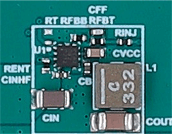
The control architecture and feature set are designed for an ultra-small design size. The device uses peak current mode control to minimize output capacitance. The LMR436x0-Q1 minimizes input filter size by using dual random spread spectrum, a low-EMI HotRod package, and an optimized pinout. The MODE/SYNC and RT pin variants can be used to set or synchronize the frequency between 200kHz and 2.2MHz to avoid noise sensitive frequency bands.
The rich feature set of the LMR436x0-Q1 is designed to simplify implementation for a wide range of automotive end equipments.
| PART NUMBER(3) | RATED CURRENT | PACKAGE (1) | PACKAGE SIZE(2) |
|---|---|---|---|
| LMR43620-Q1 | 2A | RPE (VQFN-HR, 9) | 2.00mm × 2.00mm |
| LMR43610-Q1 | 1A |
 Typical Design Size (10mm × 10mm)
 Efficiency: VOUT = 3.3V (Fixed),
2.2MHz