SNVSBE0G October   2020  – May 2024 LMR43610-Q1 , LMR43620-Q1

PRODUCTION DATA  

  1.   1
  2. Features
  3. Applications
  4. Description
  5. Device Comparison Table
  6. Pin Configuration and Functions
  7. Specifications
    1. 6.1 Absolute Maximum Ratings
    2. 6.2 ESD Ratings
    3. 6.3 Recommended Operating Conditions
    4. 6.4 Thermal Information
    5. 6.5 Electrical Characteristics
    6. 6.6 System Characteristics
    7. 6.7 Typical Characteristics
  8. Detailed Description
    1. 7.1 Overview
    2. 7.2 Functional Block Diagram
    3. 7.3 Feature Description
      1. 7.3.1  Enable, Start-Up, and Shutdown
      2. 7.3.2  External CLK SYNC (with MODE/SYNC)
        1. 7.3.2.1 Pulse-Dependent MODE/SYNC Pin Control
      3. 7.3.3  Adjustable Switching Frequency (with RT)
      4. 7.3.4  Power-Good Output Operation
      5. 7.3.5  Internal LDO, VCC, and VOUT/FB Input
      6. 7.3.6  Bootstrap Voltage and VBOOT-UVLO (BOOT Terminal)
      7. 7.3.7  Output Voltage Selection
      8. 7.3.8  Spread Spectrum
      9. 7.3.9  Soft Start and Recovery from Dropout
        1. 7.3.9.1 Recovery from Dropout
      10. 7.3.10 Current Limit and Short Circuit
      11. 7.3.11 Thermal Shutdown
      12. 7.3.12 Input Supply Current
    4. 7.4 Device Functional Modes
      1. 7.4.1 Shutdown Mode
      2. 7.4.2 Standby Mode
      3. 7.4.3 Active Mode
        1. 7.4.3.1 CCM Mode
        2. 7.4.3.2 Auto Mode – Light-Load Operation
          1. 7.4.3.2.1 Diode Emulation
          2. 7.4.3.2.2 Frequency Reduction
        3. 7.4.3.3 FPWM Mode – Light-Load Operation
        4. 7.4.3.4 Minimum On-Time (High Input Voltage) Operation
        5. 7.4.3.5 Dropout
  9. Application and Implementation
    1. 8.1 Application Information
    2. 8.2 Typical Application
      1. 8.2.1 Design Requirements
      2. 8.2.2 Detailed Design Procedure
        1. 8.2.2.1  Choosing the Switching Frequency
        2. 8.2.2.2  Setting the Output Voltage
          1. 8.2.2.2.1 FB for Adjustable Output
        3. 8.2.2.3  Inductor Selection
        4. 8.2.2.4  Output Capacitor Selection
        5. 8.2.2.5  Input Capacitor Selection
        6. 8.2.2.6  CBOOT
        7. 8.2.2.7  VCC
        8. 8.2.2.8  CFF Selection
        9. 8.2.2.9  External UVLO
        10. 8.2.2.10 Maximum Ambient Temperature
      3. 8.2.3 Application Curves
    3. 8.3 Best Design Practices
    4. 8.4 Power Supply Recommendations
    5. 8.5 Layout
      1. 8.5.1 Layout Guidelines
        1. 8.5.1.1 Ground and Thermal Considerations
      2. 8.5.2 Layout Example
  10. Device and Documentation Support
    1. 9.1 Device Support
      1. 9.1.1 Third-Party Products Disclaimer
      2. 9.1.2 Device Nomenclature
    2. 9.2 Documentation Support
      1. 9.2.1 Related Documentation
    3. 9.3 Receiving Notification of Documentation Updates
    4. 9.4 Support Resources
    5. 9.5 Trademarks
    6. 9.6 Electrostatic Discharge Caution
    7. 9.7 Glossary
  11. 10Revision History
  12. 11Mechanical, Packaging, and Orderable Information

Dropout

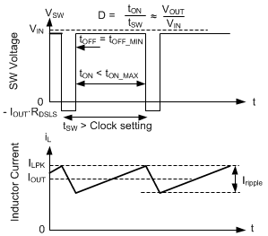
Dropout operation is defined as any input-to-output voltage ratio that requires frequency to drop to achieve the required duty cycle. At a given clock frequency, duty cycle is limited by minimum off time. After this limit is reached as shown in Figure 7-21 if clock frequency was to be maintained, the output voltage falls. Instead of allowing the output voltage to drop, the LMR436x0-Q1 extends the high-side switch on time past the end of the clock cycle until the needed peak inductor current is achieved. The clock is allowed to start a new cycle after peak inductor current is achieved or after a pre-determined maximum on time, tON-MAX, of approximately 9µs passes. As a result, after the needed duty cycle cannot be achieved at the selected clock frequency due to the existence of a minimum off time, frequency drops to maintain regulation. As shown in Figure 7-20, if input voltage is low enough so that output voltage cannot be regulated even with an on time of tON-MAX, output voltage drops to slightly below the input voltage by VDROP. For additional information on recovery from dropout, refer to Figure 7-11.

LMR43610-Q1 LMR43620-Q1 Frequency and Output Voltage
                    in Dropout
Output voltage and frequency versus input voltage: If there is little difference between input voltage and output voltage setting, the IC reduces frequency to maintain regulation. If input voltage is too low to provide the desired output voltage at approximately 110kHz, input voltage tracks output voltage.
Figure 7-20 Frequency and Output Voltage in Dropout
LMR43610-Q1 LMR43620-Q1 Dropout Waveforms
Switching waveforms while in dropout. Inductor current takes longer than a normal clock to reach the desired peak value. As a result, frequency drops. This frequency drop is limited by tON-MAX.
Figure 7-21 Dropout Waveforms