SNVSBE0G October 2020 – May 2024 LMR43610-Q1 , LMR43620-Q1
PRODUCTION DATA
- 1
- 1 Features
- 2 Applications
- 3 Description
- 4 Device Comparison Table
- 5 Pin Configuration and Functions
- 6 Specifications
-
7 Detailed Description
- 7.1 Overview
- 7.2 Functional Block Diagram
- 7.3
Feature Description
- 7.3.1 Enable, Start-Up, and Shutdown
- 7.3.2 External CLK SYNC (with MODE/SYNC)
- 7.3.3 Adjustable Switching Frequency (with RT)
- 7.3.4 Power-Good Output Operation
- 7.3.5 Internal LDO, VCC, and VOUT/FB Input
- 7.3.6 Bootstrap Voltage and VBOOT-UVLO (BOOT Terminal)
- 7.3.7 Output Voltage Selection
- 7.3.8 Spread Spectrum
- 7.3.9 Soft Start and Recovery from Dropout
- 7.3.10 Current Limit and Short Circuit
- 7.3.11 Thermal Shutdown
- 7.3.12 Input Supply Current
- 7.4 Device Functional Modes
-
8 Application and Implementation
- 8.1 Application Information
- 8.2
Typical Application
- 8.2.1 Design Requirements
- 8.2.2 Detailed Design Procedure
- 8.2.3 Application Curves
- 8.3 Best Design Practices
- 8.4 Power Supply Recommendations
- 8.5 Layout
- 9 Device and Documentation Support
- 10Revision History
- 11Mechanical, Packaging, and Orderable Information
7.4.3.1 CCM Mode
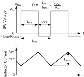
The following operating description of the LMR436x0-Q1 refers to Section 7.2 and to the waveforms in Figure 7-15. In CCM, the LMR436x0-Q1 supplies a regulated output voltage by turning on the internal high-side (HS) and low-side (LS) switches with varying duty cycle (D). During the HS switch on time, the SW pin voltage, VSW, swings up to approximately VIN, and the inductor current, iL, increases with a linear slope. The HS switch is turned off by the control logic. During the HS switch off time, tOFF, the LS switch is turned on. Inductor current discharges through the LS switch, which forces the VSW to swing below ground by the voltage drop across the LS switch. The converter loop adjusts the duty cycle to maintain a constant output voltage. D is defined by the on time of the HS switch over the switching period:
In an ideal buck converter where losses are ignored, D is proportional to the output voltage and inversely proportional to the input voltage:
 Figure 7-15 SW Voltage and Inductor Current Waveforms in Continuous Conduction Mode (CCM)